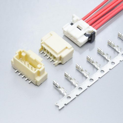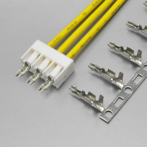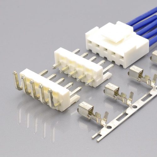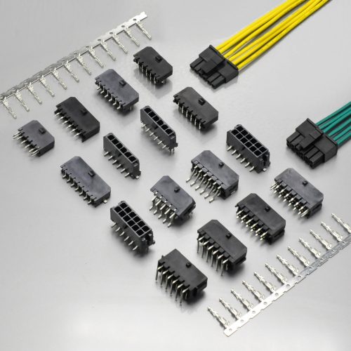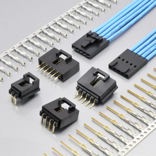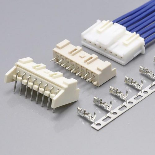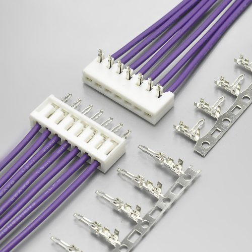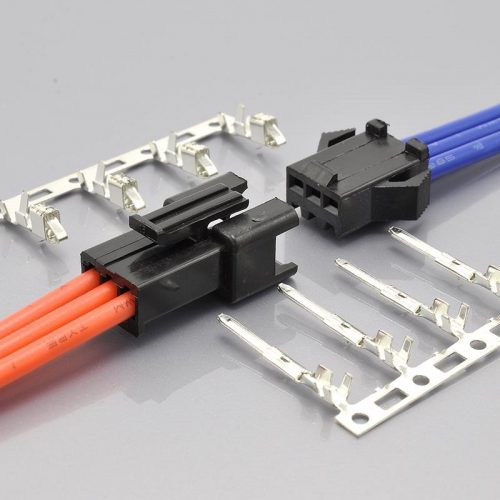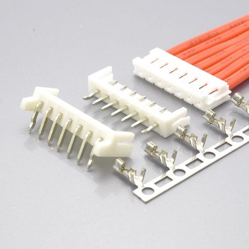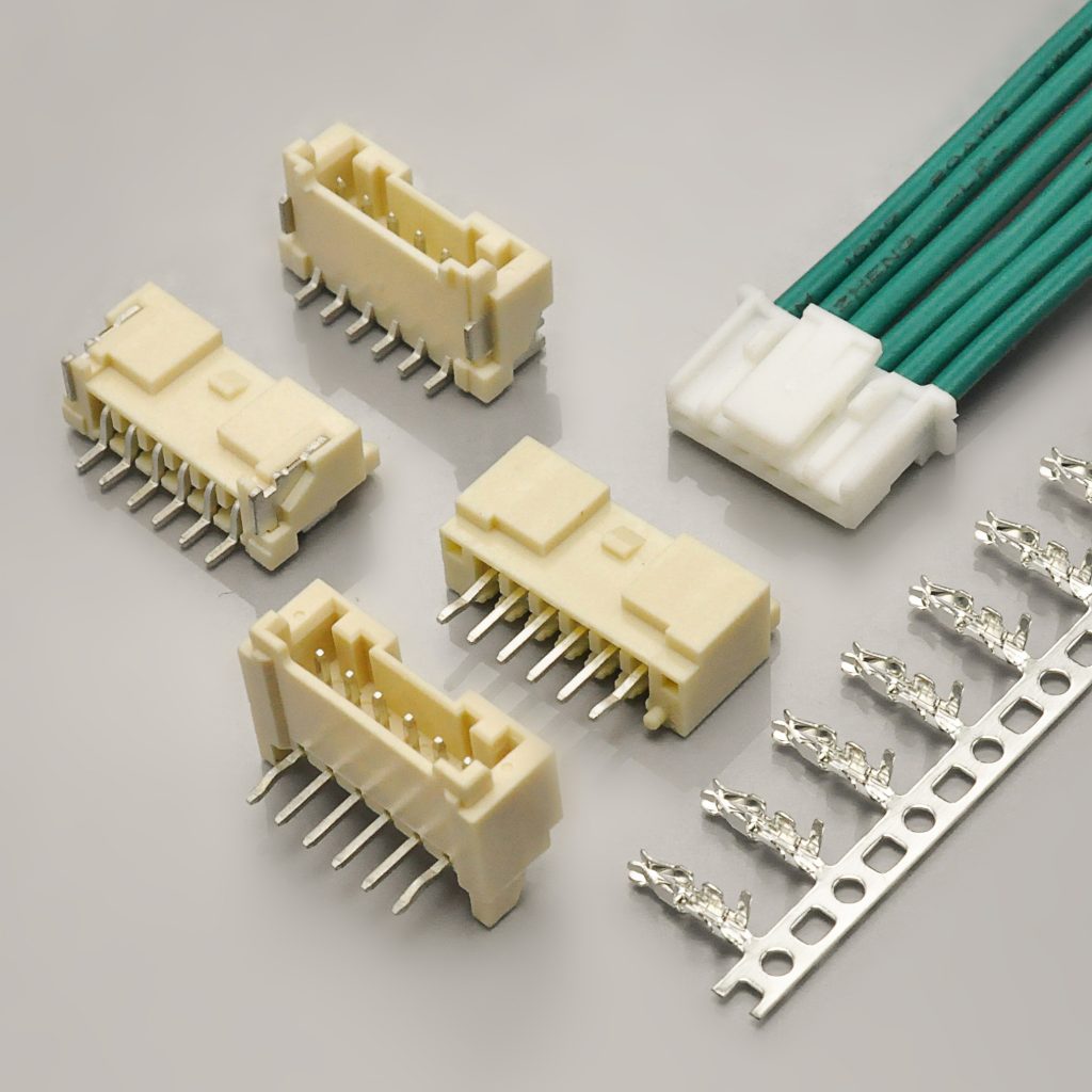
Quick answer: A JST PA 2.0 connector is a single-row, 2.0mm-pitch crimp connector family with a secure locking mechanism, built from PAP housings, PASK through-hole headers and PASS surface-mount headers. The standard PA type is rated 3A AC/DC at AWG #22, 250V AC/DC, −40°C to +105°C, over 2 to 16 circuits. The KONNRA KR2014 is its cross-reference equivalent across 2 to 15 circuits at the same 2.00mm pitch, 3A and 250V.
Two things on the JST side decide whether this replacement actually works for you, and neither is visible from the headline numbers.
The first: “JST PA 2.0” is not one specification. It is three. The catalogue publishes a separate ratings block for each variant, and they do not agree:
| JST PA variant | Voltage rating | Temperature range |
|---|---|---|
| PA standard type (retainer non-compatible) | 250V AC/DC | −40°C to +105°C |
| PA retainer-compatible type | 100V AC/DC | −40°C to +105°C |
| PAL (wire-to-wire) | 100V AC/DC | −25°C to +85°C |
So “JST PA 2.0 — 250V, −40 to +105°C” is only true of one of the three variants. If your design uses the retainer-compatible housing, or the wire-to-wire PAL, the voltage rating is 100V — not 250V — and the PAL’s usable range is −25°C to +85°C against the standard type’s −40°C to +105°C — 15°C short at the cold end and 20°C at the hot end. Quoting the family’s best number as if it applied to every variant is the single easiest mistake to make here.
The second: the 3A rating is earned on a wire gauge the KR2014 does not offer. JST’s PA family covers AWG #28 to #22, and its 3A rating is specified at AWG #22. The KR2014 covers AWG #24 to #28 — #22 is absent entirely, and its 3A is specified at #24. Section 2 below sets out why that is not a small difference.
Everything here is drawn from JST’s official PA-family catalogue and KONNRA’s specification and component pages, all cited at the end.
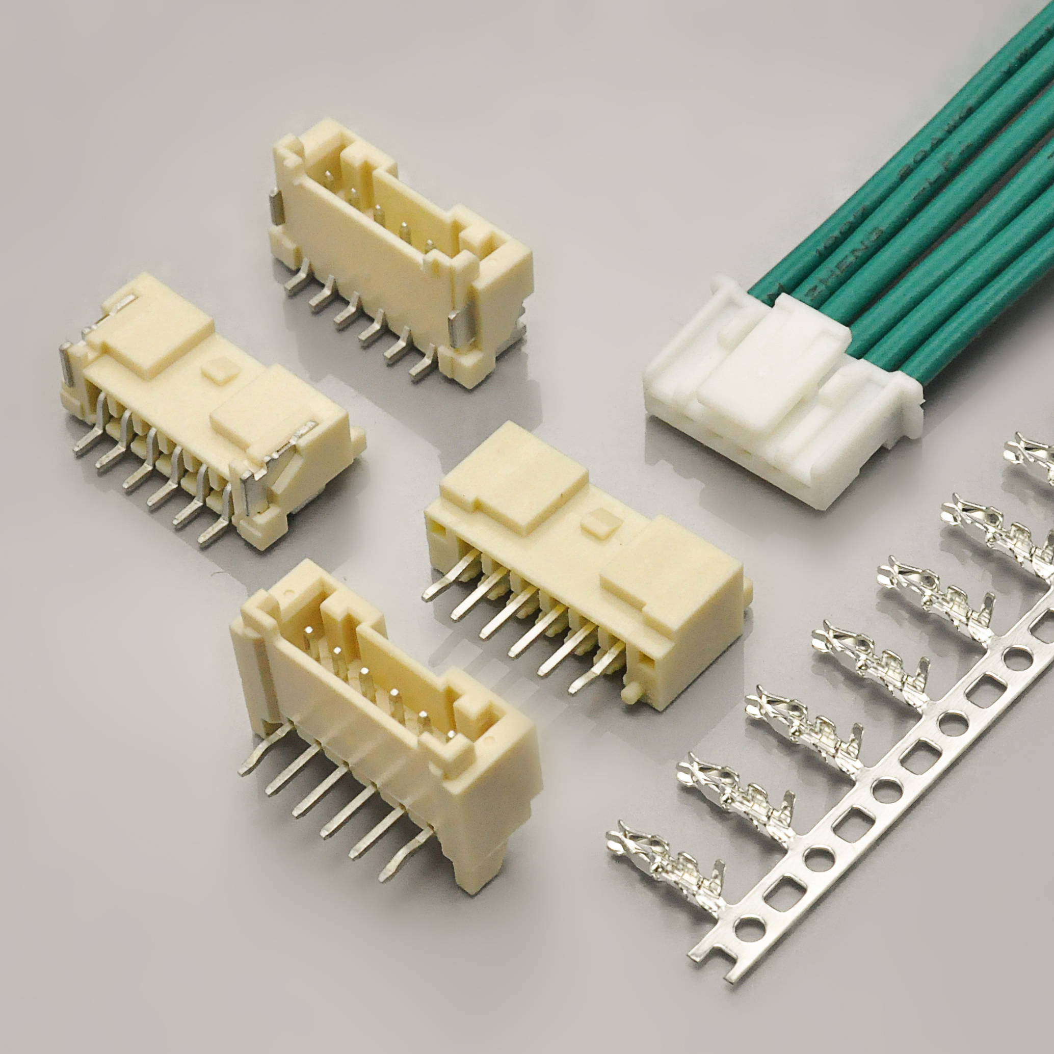
KONNRA KR2014 series PA 2.0 wire-to-board cable connector, the cross-reference equivalent for the JST PA family
At a glance
| Item | JST PA family | KONNRA KR2014 |
|---|---|---|
| Pitch | 2.0mm | 2.00mm |
| Rows | Single row | Single row |
| Circuits | 2–16 (standard PA housing and PASK header) | 2–15 (all four wafer types) |
| Application | Wire-to-board (PA), wire-to-wire (PAL) | Wire-to-board |
| Current, standard type | 3A AC/DC at AWG #22 | 3A at 24 AWG |
| Voltage, standard PA | 250V AC/DC | 250V AC/DC |
| Voltage, retainer-compatible PA | 100V AC/DC | not applicable |
| Voltage, PAL | 100V AC/DC | not applicable |
| Operating temperature, PA | −40°C to +105°C | −40°C to +105°C |
| Operating temperature, PAL | −25°C to +85°C | not applicable |
| Contact resistance | 10mΩ initial / 20mΩ after test (standard PA) | 20mΩ initial / 40mΩ after test |
| Insulation resistance | 1,000MΩ min | 1,000MΩ min |
| Withstanding voltage | 800VAC for 1 minute | 800V AC/minute |
| Applicable wire | AWG #28 to #22 | AWG #24 to #28 |
| Insulation outside diameter | φ0.76mm to φ1.5mm | 0.90 to 1.40mm |
| Housing material | PA (grade by variant) | PA66, UL94V-0 |
| Header base material | PBT (GF) through-hole; PA (heat resistance) SMT | PA9T or LCP, UL94 V-0 |
| Header post / contact material | Copper alloy, tin-plated | Brass, matte-tin over nickel |
| Locking | Secure locking mechanism | Safety locking device |
| Retainer option | Yes — three retainer versions | Not published |
| RoHS | RoHS2 compliant | RoHS compliant (stated on the product page) |
Four rows in that table need a note before you build on them.
The circuits row is not symmetrical, and it cuts both ways. JST’s standard PA housing (PAP) runs 2–16, and its through-hole header (PASK) also runs 2–16. KONNRA stops at 15. But JST’s surface-mount header (PASS) runs 2–15 with 14 circuits missing from the catalogue table. So the KR2014 can supply a 14-circuit SMT header that JST’s own PASS table does not list — an advantage in one direction and a shortfall in the other. Neither side covers everything the other does.
The contact-resistance row is where the replacement is measurably looser, at both ends. JST’s standard PA type is 10mΩ max initially and 20mΩ max after test. The KR2014 is 20mΩ max initially and 40mΩ max after test — double the original at both points. That is not a rounded-up comparison; both figures are published, and it means a circuit budget sized on the JST number does not transfer.
The header base material is a different family, not a different grade. JST builds the through-hole header from PBT (GF) and the SMT header from a heat-resistant PA. KONNRA builds both from PA9T or LCP. Read that “or” carefully — see the materials section below, because the specification leaves the choice open while the product page names only one.
The retainer row is a range gap, not a specification gap. JST’s PA family offers three retainer versions depending on the application, and the retainer-compatible housings take a different contact (SPA-001T-P0.5) on a narrower wire range. KONNRA’s KR2014 documents no retainer. If your design relies on one, this series is not a substitute for that part of the family.
“JST PA 2.0” is three specifications, not one
This is the finding that changes how you read every other PA datasheet you have, so it is worth setting out in full.
JST publishes the PA family as one catalogue with three separate specification blocks. They differ in voltage, in temperature, in contact resistance and in wire range:
| Parameter | PA standard type | PA retainer-compatible type | PAL (wire-to-wire) |
|---|---|---|---|
| Current rating | 3A AC/DC at AWG #22 | 3A AC/DC at AWG #22 | 3A AC/DC at AWG #22 |
| Voltage rating | 250V AC/DC | 100V AC/DC | 100V AC/DC |
| Temperature range | −40°C to +105°C | −40°C to +105°C | −25°C to +85°C |
| Contact resistance, initial | 10mΩ max | 15mΩ max | 15mΩ max |
| Contact resistance, after test | 20mΩ max | 25mΩ max | 25mΩ max |
| Insulation resistance | 1,000MΩ min | 1,000MΩ min | 1,000MΩ min |
| Withstanding voltage | 800VAC for 1 minute | 800VAC for 1 minute | 800VAC for 1 minute |
| Applicable wire | AWG #28 to #22 | AWG #26 to #22 | AWG #28 to #22 |
| Insulation O.D. | φ0.76 to φ1.5mm | φ0.9 to φ1.5mm | φ0.9 to φ1.5mm |
| Extra published limit | — | PC board thickness 1.6mm | Panel thickness 0.5 to 2.0mm |
Three things follow, and each one has cost a designer a re-spin somewhere.
The voltage rating drops from 250V to 100V when you move to the retainer-compatible variant. That is a factor of 2.5, and the two variants are sold under the same “PA 2.0” name, mate with the same headers, and share the same 3A current rating. Nothing about the part number prefix tells you the voltage changed — you have to know which rating block applies. A 250V-rated design that quietly migrates to a retainer-compatible housing is a 100V design.
PAL is a narrower part than “PA 2.0” suggests. It is the wire-to-wire member of the family, and its published envelope is 100V and −25°C to +85°C — both the voltage and the temperature range are reduced relative to the standard PA. If a requirement calls for a −40°C cold end and the connector is a PAL, the part cannot meet it. Note also that PAL is the one that mates with PA connectors, so a wire-to-wire run and a wire-to-board run in the same harness can have different ratings at each end.
The contact-resistance limits are not family-wide either. The standard type is 10mΩ initial / 20mΩ after test; the other two variants are 15mΩ / 25mΩ. The catalogue does not explain why the retainer-compatible design is 50% higher, and it may simply reflect a different contact geometry — but it means you cannot carry a contact-resistance budget across variants any more than you can carry a voltage rating.
Which one applies to your design
JST’s naming gives you the answer if you know where to look:
| Variant | Housing prefix | Contact prefix |
|---|---|---|
| PA standard (retainer non-compatible) | PAP | SPHD |
| PA retainer-compatible | PARP and PMS | SPA |
| PAL wire-to-wire | PAL / see the PAL housing table | SPAL |
So a PAP housing is the 250V variant; a PARP or PMS housing is the 100V one; and SPAL contacts mean you are in the wire-to-wire branch. Reading the prefix settles the rating question in one step.
The AWG #22 gap: the 3A rating is earned on different wire
Both parts say 3A. Only one of them reaches 3A on the wire you are probably using.
| JST PA standard type | KONNRA KR2014 | |
|---|---|---|
| Applicable conductor range | AWG #28 to #22 | AWG #24 to #28 |
| Gauge at which 3A is specified | AWG #22 | AWG #24 |
| 22 AWG supported? | Yes | No |
| Insulation O.D. range | φ0.76 to φ1.5mm | 0.90 to 1.40mm |
| Contacts needed to cover the range | Two — SPHD-002T-P0.5 and SPHD-001T-P0.5 |
One — a single terminal part number |
KONNRA’s published wire range starts at AWG #24, so AWG #22 is not a documented option at all. There is no 22 AWG row in the crimp table, and the specification’s applicable-wire line reads AWG 24# to 28#. A harness built on 22 AWG — which is exactly the wire that gives the PA family its 3A rating — cannot be crimped onto a KR2014 terminal.
And the reason becomes obvious when you look at how JST assembles its own wire range. JST does not use one contact for #28–#22; it uses two:
| JST contact | Conductor range | Insulation O.D. | Qty/reel |
|---|---|---|---|
SPHD-002T-P0.5 |
#28 to #24 (0.08 to 0.21 mm²) | 0.76 to 1.5mm | 8,000 |
SPHD-001T-P0.5 |
#26 to #22 (0.13 to 0.33 mm²) | 1.0 to 1.5mm | 8,000 |
The range is split because a single crimp barrel cannot hold 0.08mm² and 0.33mm² wire with equal reliability. The KR2014’s single terminal sits at the SPHD-002T-P0.5 end of that table — its documented range (#24–#28) matches the first contact almost exactly, and it does not reach the second.
So the precise statement is this: the KR2014 is a substitute for the SPHD-002T-P0.5 branch of the PA family, and has no equivalent for the SPHD-001T-P0.5 branch. And the -001 contact is the one that carries the headline 3A.
What that means for the current rating, stated carefully. Both documents say 3A, and I am not claiming either is wrong. But the 3A is being carried by a thinner conductor on the KONNRA side: 24 AWG (≈0.205mm²) rather than 22 AWG (≈0.326mm²). The same current through a smaller cross-section means higher current density and more self-heating in the wire, and the specification’s own 30°C maximum temperature rise is the limit that governs — measured at rated current, in the assembly’s own thermal environment. So the right question is not “does it say 3A?” but “at 3A on my actual gauge, does the assembly stay inside a 30°C rise?” That is a bench measurement, and it is the first thing to test on a first article.
One further practical consequence: the insulation diameter window is narrower on the KONNRA side — 0.90 to 1.40mm against JST’s 0.76 to 1.50mm. A wire that sits comfortably inside the JST window may be outside the KONNRA one at either end, and the relevant number for a given gauge is the insulation diameter, not the conductor gauge. Check the actual wire you are using, not the AWG stamp on it.
The six KONNRA component pages disagree with each other and with the specification
KONNRA documents this series on a product page, a seven-page specification, a series drawing, and six per-component pages — housing, terminal, and four wafers. Read together, they contain four defects: three contradictions of fact, and one misdirected link that can cost you a design.
Contradiction one: three different wire ranges
| Source | Wire size as published |
|---|---|
| Housing component page | 20#-24# |
| Terminal component page | 24# |
| All four wafer component pages | 24# each |
Specification PS-KR2014-01, section 4.0 |
AWG 24# ~ 28# |
| Product page | #24~#28 |
Three mutually incompatible answers to one question. The specification and the product page agree on #24–#28. Every component page except the housing reduces that to a single value, #24. And the housing page claims #20–#24 — a range that overlaps the others at exactly one gauge and extends three sizes larger.
The housing page is the problem. AWG #20 is a 0.52mm² conductor — more than twice the copper of 24 AWG — and it is a much larger wire than a 2.0mm-pitch, 3A crimp system carries. The specification’s crimp table has no 20 AWG row, and the terminal’s own published range starts at #24. So the housing page’s “20#-24#” cannot be satisfied by any terminal in the series.
Two consequences worth naming. First, an engineer filtering the KONNRA catalogue by wire gauge will find the KR2014 housing under AWG 20 and reasonably conclude the series takes that wire; it does not. Second, the housing page and the terminal page — two pages describing the two halves of one mating pair — do not agree on what wire the pair accepts, which is precisely the pair of documents a designer reads together.
Use #24–#28 from the specification, and treat the housing page’s 20#-24# as an error to be corrected.
Contradiction two: the housing page publishes the original’s contact resistance
| Source | Contact resistance as published |
|---|---|
| Housing component page | 10mΩMax |
| Terminal and all four wafer pages | 20mΩMax |
| Specification | 20mΩ max initial, 40mΩ max after environmental test |
The housing page is the only document in the entire KR2014 set that says 10mΩ. Every other page says 20mΩ, and the specification says 20mΩ as the initial limit.
It is worth pausing on what 10mΩ is: 10mΩ is JST’s figure. The JST PA standard type is specified at 10mΩ initial. So the KR2014 housing page appears to have inherited the original manufacturer’s number rather than KONNRA’s own — and it happens to be the more attractive figure of the two.
Design against 20mΩ initial and 40mΩ after test. Those are the numbers in the specification, and they are the ones the other five pages and the test programme support.
Contradiction three: six pages, six phrasings of the same cross-reference
Every one of the six component pages names a JST family it is compatible with. No two of them phrase it the same way:
| KONNRA component page | “Compatible” field as published |
|---|---|
| Housing | PAP Series |
| Terminal | PA2.0 Series |
| DIP Right Angle Wafer | S**B PASK Series |
| SMT Right Angle Wafer | SM**B PASS Series |
| DIP Straight Wafer | B**B-PASK Series |
| SMT Straight Wafer | BM**B PASS Series |
This one is a documentation problem rather than an engineering one, and it is worth saying so plainly, because the underlying mapping is correct. Checked against JST’s own part-number structure, all four wafer mappings land on the right JST parts:
| KONNRA wafer | JST equivalent | Does the geometry agree? |
|---|---|---|
DIP Straight (vd-wafer) |
B**B-PASK — PASK top entry, through-hole |
Yes |
DIP Right Angle (rd-wafer) |
S**B PASK — PASK side entry, through-hole |
Yes |
SMT Straight (vs-wafer) |
BM**B PASS — PASS top entry, SMT |
Yes |
SMT Right Angle (rs-wafer) |
SM**B PASS — PASS side entry, SMT |
Yes |
Straight maps to top entry, right angle maps to side entry, and the through-hole/SMT split maps to PASK/PASS. Every mapping is correct. Only the wording varies — one page says “PA2.0 Series” where the others name a specific JST prefix, and the asterisk conventions differ between pages.
That is worth stating as a positive: this series’ cross-reference is semantically right and cosmetically inconsistent, which is a much better failure mode than the reverse. But if you are quoting a compatible part number to a customer, take it from the row above rather than from whichever component page you happened to open.
And one page links to the wrong series’ drawing
A concrete defect with a direct cost, so it gets its own mention.
The DIP Straight Wafer page’s “Series Drawing” link points at KR2022-series-drawing.pdf.
KR2022 is a different connector series — a different pitch family and a different JST cross-reference. So a designer who opens the KR2014 DIP straight wafer page, trusts the “Series Drawing” button, and downloads the file gets a drawing for a part they are not looking at. The other five component pages link to the correct KR2014-Series-Drawing.pdf.
The failure mode is quiet: the file downloads, it is a valid drawing, and it carries a KR-series header. Only the part geometry is wrong. If you have already pulled a KR2014 straight-DIP wafer drawing, re-pull it from the product page link rather than the component page.
Where the two systems match
Strip out the variant differences and the overlap on the standard PA type is substantial.
| Parameter | JST PA standard type | KONNRA KR2014 | Match |
|---|---|---|---|
| Pitch | 2.0mm | 2.00mm | Exact |
| Rows | Single row | Single row | Exact |
| Application | Wire-to-board | Wire-to-board | Exact |
| Voltage rating | 250V AC/DC | 250V AC/DC | Exact |
| Withstanding voltage | 800VAC / 1 minute | 800V AC/minute | Exact |
| Insulation resistance | 1,000MΩ min | 1,000MΩ min | Exact |
| Temperature range | −40°C to +105°C | −40°C to +105°C | Exact |
| Contact material | Copper alloy, tin-plated | Brass, matte-tin over nickel | Equivalent |
| Locking feature | Secure locking mechanism | Safety locking device | Equivalent function |
| RoHS | RoHS2 compliant | RoHS compliant | Both compliant |
Three of those rows deserve more than a tick.
The temperature range matching at both ends is the strongest single point in this comparison. Unlike some other series in this catalogue, the cold end is not narrowed: −40°C to +105°C on both sides, which means a design qualified against the JST range transfers without re-qualification on thermal grounds. Confirm the variant first, though — a PAL is only −25°C to +85°C, so a harness that mixes PA and PAL has two different thermal envelopes in it.
The contact materials match in family, and the plating differs in a way worth knowing. JST specifies copper alloy, tin-plated; KONNRA specifies brass, matte-tin over nickel. Brass is a copper alloy, so the substrate is equivalent. But two details differ: KONNRA adds a nickel barrier layer under the tin — the layer that keeps the tin from diffusing into the substrate over temperature, and a genuinely better construction at +105°C — and specifies matte tin rather than bright tin. Matte tin is the whisker-resistant finish, and its inclusion is a point in the KR2014’s favour. JST’s catalogue states “tin-plated” without naming the matte/bright distinction or a nickel underlayer.
The current rating is the row where the two columns look identical and are not. Both say 3A. They are specified at different wire gauges — #22 against #24 — and that is the subject of the section above.
Where the two systems differ
| Parameter | JST PA standard type | KONNRA KR2014 | Nature of the difference |
|---|---|---|---|
| Contact resistance, initial | 10mΩ max | 20mΩ max | 2× looser |
| Contact resistance, after test | 20mΩ max | 40mΩ max | 2× looser |
| Applicable wire | #28 to #22 | #24 to #28 | #22 absent |
| Insulation O.D. | φ0.76 to φ1.5mm | 0.90 to 1.40mm | Narrower both ends |
| Circuits | 2–16 | 2–15 | KONNRA stops one short |
| SMT header circuits | 2–15, 14 missing | 2–15, continuous | KONNRA covers 14 |
| Header base material | PBT (GF) / heat-resistant PA | PA9T or LCP | Different family, open choice |
| Terminal plating options | Tin-plated | Tin/Gold on terminal | KONNRA offers gold |
| DIP wafer contact plating | Tin-plated | Matte-tin or gold over nickel | KONNRA offers gold |
| SMT wafer contact plating | Tin-plated | Matte-tin only | No gold on SMT |
| Retainer | Three retainer versions | Not published | Range gap |
| PCB thickness | 1.6mm (retainer-compatible type) | Not published | Gap |
| Panel thickness | 0.5–2.0mm (PAL) | Not applicable | Different product |
Four of those differences deserve more than a table cell.
The contact resistance is double the original, and it is a published figure on both sides
JST: 10mΩ max initial, 20mΩ max after test. KONNRA: 20mΩ max initial, 40mΩ max after test.
This is a clean, doubling, like-for-like difference — both manufacturers publish both an initial and a post-test limit, and both use the same test basis (dry circuit, EIA-364-23C). There is no ambiguity in it and no way to read the two as equivalent.
Where it matters is a circuit carrying a low-level signal, or a design with a specified total loop resistance across a mated pair and a length of cable. 20mΩ per contact against a 10mΩ budget is 10mΩ of unplanned resistance, and it doubles again after environmental conditioning. For power circuits at 3A it is immaterial — 20mΩ at 3A is 0.18V and 0.54W across the pair, and the specification’s 30°C maximum rise governs instead. For signal circuits it is the number to check first.
The header base material is an open choice on one side and a fixed one on the other
KONNRA’s specification section 3.0 states the wafer base as “PA9T or LCP” for both the SMT and DIP types. The product page states “PA9T” alone, and all four wafer component pages state “Nylon 9T” — which is PA9T, so the pages agree with each other and with one of the two options the specification permits.
So the specification allows either of two base resins, and no other document narrows it. PA9T and LCP are both high-temperature crystalline polymers suitable for soldering, but they are not interchangeable in a design review: they differ in coefficient of thermal expansion, in moisture uptake, and in cost. If your application has a specified base material, or if the thermal-cycling behaviour of the soldered joint matters, “PA9T or LCP” is not an answer — it is a question to put to the supplier before qualification.
By contrast, JST names a single material for each header type: PBT (GF) for the through-hole header and a heat-resistant PA for the SMT header. Neither is PA9T or LCP, so this is a genuine change of material family rather than a grade substitution — and note that the through-hole and SMT headers are different materials from each other on the JST side, which is not a distinction the KR2014 makes.
Gold plating is available on some components and not others
This one is easy to get wrong when specifying, so it is worth laying out exactly.
| Component | KONNRA plating as specified |
|---|---|
| Terminal (crimp contact) | Tin/Gold plated over nickel |
| DIP wafer contact | Matte-Tin/Gold plated over nickel |
| SMT wafer contact | Matte-Tin only — no gold option |
| SMT wafer solder tab | Matte-Tin over nickel |
A gold board interface is available on the through-hole wafer but not on the surface-mount one. The specification is explicit about this — the SMT block lists “Matte-Tin Plated Over Nickel” for the contact where the DIP block lists “Matte-Tin/Gold” — and all four wafer component pages show only “Tin over Nickel”, which under-reports the gold option that exists on the DIP part.
So: if your design needs a gold-plated mating interface at the board, it must be a DIP wafer. A gold-on-both-sides specification cannot be met with the KR2014 SMT wafers, and the component pages will not tell you that, because they show tin on all four.
JST’s PA contacts in this catalogue are tin-plated, so a gold interface is an option the KR2014 offers that the original does not — but only on half the wafer range.
The circuit ranges differ in both directions
| Series | 14 circuits | 16 circuits |
|---|---|---|
| JST PAP housing (through-hole family) | Listed | Listed |
| JST PASK header (through-hole) | Listed | Listed |
| JST PASS header (SMT) | Not listed | Not listed |
| KONNRA KR2014 (all four wafers) | Listed | Not available |
JST’s standard PA runs to 16 circuits; the KR2014 stops at 15. If your board has sixteen positions, no KR2014 wafer or housing covers it and the design needs a formal review rather than a substitution.
But JST’s own SMT header table skips 14. The PASS series is published for 2 through 13 and then 15 — fourteen circuits is absent from that table, while it is present in the PASK through-hole table and in both PAP and PARP housings. The KR2014 lists 14 circuits across all four wafer types, so a fourteen-position surface-mount design that JST’s catalogue does not cover is available from KONNRA.
Neither direction is a defect. The point is that “2–15 versus 2–16” understates what is going on: the two ranges are not nested, and each side covers a size the other does not.
The force table: two exact laws and a constant loss
Section 8.0 of the KONNRA specification publishes insertion and withdrawal force for every circuit count from 2 to 15, at initial and after 30 mating cycles. Units are kgf.
| Circuits | 2 | 3 | 4 | 5 | 6 | 7 | 8 | 9 | 10 | 11 | 12 | 13 | 14 | 15 |
|---|---|---|---|---|---|---|---|---|---|---|---|---|---|---|
| I.F. max | 1.5 | 2.0 | 2.5 | 3.0 | 3.5 | 4.0 | 4.5 | 5.0 | 5.5 | 6.0 | 6.5 | 7.0 | 7.5 | 8.0 |
| R.F. min, initial | 0.20 | 0.30 | 0.40 | 0.50 | 0.60 | 0.70 | 0.80 | 0.90 | 1.00 | 1.10 | 1.20 | 1.30 | 1.40 | 1.50 |
| R.F. min, after 30 cycles | 0.15 | 0.25 | 0.35 | 0.45 | 0.55 | 0.65 | 0.75 | 0.85 | 0.95 | 1.05 | 1.15 | 1.25 | 1.35 | 1.45 |
Both laws reproduce every published value
I.F. = 0.50 + 0.50 × circuits — 0.50 + 1.00 = 1.5 at two circuits, 0.50 + 7.50 = 8.0 at fifteen. R.F. = 0.10 × circuits — 0.20 at two circuits, 1.50 at fifteen.
All twenty-eight published values across the two rows follow these two relations with no exception anywhere in the table. Two things follow from the shapes.
Insertion force has a fixed 0.50 kgf of housing engagement plus 0.50 kgf per contact. The constant per-contact term means a two-circuit sample predicts the fifteen-circuit force exactly, so worst-case insertion force does not need to be measured — only calculated. There is no friction penalty for adding positions.
Withdrawal force is purely per-contact, with no baseline term at all. R.F. = 0.10 × circuits means the housing’s own engagement contributes nothing to holding force — the retention is entirely the sum of the contacts. That is the cleanest possible form for an interconnect, and it means retention scales linearly with no size where the design changes character.
The per-contact relationship between the two is also fixed: withdrawal is exactly 20% of insertion (0.10 against 0.50) at every size.
The loss after 30 cycles is a constant 0.05 kgf
| Circuits | 2 | 3 | 4 | 5 | 6 | 7 | 8 | 9 | 10 | 11 | 12 | 13 | 14 | 15 |
|---|---|---|---|---|---|---|---|---|---|---|---|---|---|---|
| Loss after 30 cycles (kgf) | 0.05 | 0.05 | 0.05 | 0.05 | 0.05 | 0.05 | 0.05 | 0.05 | 0.05 | 0.05 | 0.05 | 0.05 | 0.05 | 0.05 |
Identical in all fourteen rows — a constant absolute 0.05 kgf, not a percentage and not a growing penalty. Because it is constant rather than proportional, it bites hardest at the small sizes: 0.05 out of 0.20 is a 25% loss at two circuits, while 0.05 out of 1.50 is barely 3% at fifteen. If you are designing a two-position interconnect, a quarter of your retention is gone after 30 matings.
This table is one of the better-constructed ones in this supplier’s catalogue: all forty-two published values are reproducible from two formulas and a constant, and the after-30-cycles column is genuinely lower than the initial column rather than copied from it. It is reasonable to rely on it, including for interpolation at sizes you have not measured.
The terminal numbers put the withdrawal force in perspective
| Item | Specification section | Value |
|---|---|---|
| Terminal insertion force | 6.2 | 1.0 kgf (9.8 N) max, per terminal |
| Terminal / housing retention force | 6.3 | 1.5 kgf (14.7 N) min, per terminal |
| Pin retention force | 6.4 | 1.2 kgf (11.76 N) min, per pin |
A single terminal resists at least 1.5 kgf of axial pull. Compare that to the force needed to unmate the complete connector:
| Circuits | Whole-connector withdrawal (kgf) | Aggregate minimum terminal retention (kgf) | Ratio |
|---|---|---|---|
| 2 | 0.20 | 3.0 | 15 × |
| 8 | 0.80 | 12.0 | 15 × |
| 15 | 1.50 | 22.5 | 15 × |
The ratio is exactly 15 at every circuit count — not approximately, exactly, and for a reason worth seeing: the withdrawal force is 0.10 per contact and the retention is 1.5 per contact, so the ratio is 1.5 ÷ 0.10 = 15 regardless of how many contacts there are. The constant falls straight out of the two published figures.
Practically, this means the mating interface is always the intended release point and a wire will not pull out of the housing before the connector separates — but the margin is a factor of fifteen, not the factor of thirty-five seen on some other series in this catalogue. It is comfortable and it is not enormous.
The pin retention figure is the one to look at for SMT. At 1.2 kgf min per pin, it is the axial force required to pull a header post out of the wafer, and on a surface-mount part that load passes through the solder joint. Whether the joint survives it is a board-design question, not a connector-rating question, but 1.2 kgf per pin is the number your pad geometry has to survive.
One wording defect in that block, which matters if you are writing a test procedure from the document: section 6.4’s Chinese text says the pin is pulled out; the English in the same cell says “Apply axial push force.” The item measures retention, so pull-out is the sensible reading — but specify the direction yourself rather than copying the English.
Crimp and terminal data
Three wire gauges, and the ladders are not uniform.
| 24 AWG | 26 AWG | 28 AWG | |
|---|---|---|---|
| Conductor crimp width | 1.40 ± 0.1 | 1.40 ± 0.1 | 1.40 ± 0.1 |
| Conductor crimp height | 0.75 ± 0.05 | 0.70 ± 0.05 | 0.60 ± 0.05 |
| Insulation crimp width | 1.60 max | 1.60 max | 1.60 max |
| Insulation crimp height | 1.55 ± 0.10 | 1.45 ± 0.10 | 1.30 ± 0.10 |
| Crimp strength, min | 3.63 kgf | 2.27 kgf | 1.36 kgf |
| Stripping length | 1.6 – 2.3 mm | 1.6 – 2.3 mm | 1.6 – 2.3 mm |
The conductor crimp height steps unevenly: 0.05mm from 24 to 26 AWG, then 0.10mm from 26 to 28 AWG. The increment doubles at the thin end. Do not set a tool by assuming three equal steps.
The insulation crimp height steps unevenly in the other direction: 0.10mm, then 0.15mm. The increment grows where the conductor increment shrank, so the two ladders move in opposition and neither can be derived from the other. Set each from its own row.
The insulation crimp tolerance is ±0.10 against the conductor’s ±0.05 — twice as loose, which is conventional for an insulation crimp and worth noting when writing a tool-verification sheet.
Crimp strength falls by a factor of 2.67 from 24 AWG to 28 AWG (3.63 down to 1.36), while the conductor cross-section falls by roughly 2.5. The pull-out requirement therefore tracks the copper closely rather than being flat — which is what you want, because a flat requirement would be trivial at 24 AWG and unachievable at 28 AWG.
The stripping window is 1.6 to 2.3 mm — a 0.7mm band, the widest in this supplier’s 2.0mm range. For reference, the adjacent series publish 1.6–2.2mm and 1.6–2.1mm. A single strip setting will serve all three gauges here, but it is not the same window as the neighbouring series, so do not carry a setting across.
Terminal reel quantity is published in the specification’s part-number table rather than on the component pages: T20050P***01A.
Materials and plating, component by component
The product page compresses this into one line — Phosphor/Bronze/PA66/PA9T — which lists two metals and two polymers without saying which component uses which. The specification resolves it:
| Component | Base material | Plating | Colour |
|---|---|---|---|
| Housing | PA66, UL94 V-0 | — | White |
| Terminal | Phosphor bronze | Tin or gold over nickel | — |
| Wafer base (both SMT and DIP) | PA9T or LCP, UL94 V-0 | — | Natural |
| Wafer contact, SMT | Brass | Matte-tin over nickel | — |
| Wafer contact, DIP | Brass | Matte-tin or gold over nickel | — |
| Solder tab, SMT wafer | Brass | Matte-tin over nickel | — |
| Solder tab, DIP wafer | None | None | — |
Three things are worth drawing out.
The DIP wafer has no solder tab, and that is correct rather than missing. A through-hole header is held by its own posts passing through the board, so it needs no separate soldered anchor. The SMT wafer is held by solder tabs plus its contacts. The specification states “None” for the DIP solder tab explicitly, which is the right way to document an intentional absence — it stops a reader wondering whether the field was left blank.
Every plated surface on the wafer gets a nickel barrier under the tin. That is stated on both wafer types and on the solder tabs, not just on the contacts. Nickel under matte tin is the construction that keeps the surface stable at +105°C, and having it specified on the solder tabs as well as the contacts is more thorough than many headers document.
The housing is white and the wafers are natural. Both are non-pigmented shades, and the difference is cosmetic rather than functional — but note that the ordering code offers a single housing material (PA66, UL94 V-0), so there is no colour option. If your assembly procedure uses colour to prevent cross-mating, this series does not support that method.
The housing part-number prefix is 2014; the terminal’s is not
One documentation anomaly worth checking before you write a purchase order.
The specification’s part-number table reads:
| Component | Part number as published |
|---|---|
| Housing | H201401**0101A |
| Terminal | T20050P***01A |
| Straight DIP wafer | C2014VD1****M01**PA |
| Right angle DIP wafer | C2014RD1****M01**PA |
| Right angle SMT wafer | C2014RS1****M01**RA |
| Straight SMT wafer | C2014VS1****M01**RA |
Five of the six carry a “2014” series prefix. The terminal carries “2005”.
There are two readings and the document does not choose between them: either the terminal is a shared part genuinely carried over from the KR2005 series — plausible, since the two series share an identical crimp-strength ladder at 24/26/28 AWG and the same wire range — or the prefix is a transcription error carried in from the template of the series it was copied from.
I am not going to guess. Quote the terminal by its full published number and ask the supplier to confirm it applies to KR2014, particularly if you are ordering the terminal separately from a kit.
One more detail from the same table, which is easy to read past: the DIP wafers end in PA and the SMT wafers end in RA. The suffix splits by soldering technology, not by mating orientation — both orientations share a suffix within each mounting type.
The environmental programme
Eleven tests, all referenced to EIA standards, and — unusually for this supplier — the contact-resistance limit is the same in every one of them.
| Test | Condition | Reference | Contact resistance limit |
|---|---|---|---|
| Durability | 30 mating cycles at ≤ 10 cycles/minute | EIA-364-09C | 40mΩ max |
| Temperature rise | At rated current load | EIA-364-70B | (30°C max instead) |
| Vibration | 1.5mm P-P, 10~55~10 Hz in 1 minute, 2 hours in each of X, Y and Z | EIA-364-28B | 40mΩ max |
| Shock | 490 m/s² (50g), 3 strokes in each of X, Y and Z | EIA-364-27B | 40mΩ max |
| Heat resistance | 105 ± 2°C for 96 hours | EIA-364-17B | 40mΩ max |
| Cold resistance | −40 ± 2°C for 96 hours | EIA-364-59 | 40mΩ max |
| Humidity | 40 ± 2°C at 90–95% RH for 96 hours | EIA-364-31B | 40mΩ max |
| Thermal shock | −40°C 30 min → room temp 5 min → +105°C 30 min → room temp 5 min, 5 cycles | EIA-364-32B | 40mΩ max |
| Salt spray | 35 ± 2°C, 5 ± 1% solution, 24 hours | EIA-364-26B | 40mΩ max |
| Solderability | 3 ± 0.5 seconds at 245 ± 5°C | EIA-364-52 | (95% wetting instead) |
| Solder heat resistance | SMT per profile 9.1; DIP per profile 9.2 | EIA-364-56D (SMT) / EIA-364-71B (DIP) | (no damage instead) |
Eight of the eleven tests state a contact-resistance limit, and all eight allow exactly the same figure: 40mΩ max. There is no split, no carve-out, and no test held to a tighter or looser number than the others.
This is worth calling out, because it is not universal in this supplier’s documentation. An adjacent series in the same catalogue permits 60mΩ after five of its tests and 40mΩ after the other three, with no stated reason. The KR2014 specification does not have that problem — the acceptance criterion is uniform, so a single post-conditioning figure of 40mΩ applies to every environmental case and to the durability cycle. For anyone writing a qualification plan, that removes a real source of ambiguity.
The relationship to the initial limit is equally clean: 20mΩ as supplied, 40mΩ after any conditioning — an exact doubling that is consistent across the whole programme. Compare it against the original: JST specifies 10mΩ initial, 20mΩ after test, so the KR2014’s post-conditioning figure is four times the JST initial figure.
Beyond the table:
| Result | Published limit |
|---|---|
| Temperature rise at rated current | 30°C max |
| Insulation resistance, initial | 1000MΩ min |
| Insulation resistance, after humidity | 100MΩ min |
| Discontinuity under vibration and shock | 1 microsecond max |
| Solderability, wetted area | 95% of immersed area free of voids and pin holes |
The temperature rise limit of 30°C max is the number the 3A rating actually rests on, and it pairs with the wire-gauge question above: the rated current is specified at 24 AWG on this part, and the acceptance criterion is that the assembly stays within a 30°C rise while carrying it. That is the measurement to make on a first article.
And the humidity test derates insulation resistance by a factor of ten — 1000MΩ min as supplied, 100MΩ min after 96 hours at 90–95% relative humidity. The product page carries a single insulation-resistance row reading “1000MΩ min” with no post-humidity figure beside it, so in a humid application the number to design against is in section 7.7, not on the product page. JST publishes 1,000MΩ min for its PA variants and does not publish a separate reduced post-humidity figure in this catalogue, so this is a KONNRA-side derating you will not find mirrored on the original’s data sheet.
The soldering profiles, and a standards split worth noticing
| SMT (reflow) | DIP (wave) | |
|---|---|---|
| Peak | 255 ± 5°C for 5–10 sec | 250°C max for 3–5 sec |
| Time at minimum temperature | 20–40 sec at min 230°C | 60–150 sec at min 217°C |
| Reflow / soak | 90–120 sec, 30 sec | 60–180 sec, 30 sec |
| Pre-heat | 150–200°C | 150–180°C |
| Solder-heat standard | EIA-364-56D | EIA-364-71B |
The two mounting types are qualified against different EIA standards — 364-56D for the reflow-soldered SMT parts and 364-71B for the wave-soldered DIP parts. That is correct engineering rather than a documentation quirk: a surface-mount header sees a reflow profile and a through-hole header sees a wave, and they are not the same thermal event. The 255°C peak applies only to the SMT wafers and the 250°C peak only to the DIP wafers — mixing them up means qualifying a part against a process it will never see.
What is not published
| Not published | Where you would expect it |
|---|---|
| Which base resin is actually supplied | The specification says the wafer base is “PA9T or LCP”. Neither the product page nor the four wafer pages narrows it — they state PA9T/Nylon 9T only. The choice is open in the controlling document. |
| A UL- or CSA-rated voltage | KONNRA publishes UL E482542 / LV 214 on all six component pages but attaches no rated voltage to the listing. The general rating is 250V; whether the agency-recognised figure is also 250V is not stated. Given that the JST family’s own voltage ratings range from 100V to 250V depending on variant, this is worth a direct question. |
| Any retainer | JST offers three retainer versions and a retainer-compatible housing variant. No retainer appears anywhere in the KR2014 documentation. |
| A PCB thickness specification | JST’s retainer-compatible PA specifies 1.6mm board thickness and PAL specifies 0.5–2.0mm panel thickness. KONNRA publishes no board or panel thickness for the KR2014, and for a through-hole part the pin length determines the boards it will sit in. |
| A gold plating thickness | The specification offers gold on the terminal and on the DIP wafer contact, with no thickness figure on either. |
| A current derating curve against circuit count | The 3A rating is per contact. No aggregate current figure or derating curve is published. |
| A readable series drawing | KR2014-Series-Drawing.pdf is published at 2.0MB, but its content is graphics rather than text and could not be extracted for this article. All dimensional and part-number information quoted here comes from the specification and the component pages. |
Two of those rows matter more than the rest.
The open resin choice is genuinely unresolved. Every other material question in this series has a single published answer. This one has two alternatives in the controlling document and one of them named everywhere else, which means the only way to know what you will receive is to ask. If LCP is not acceptable in your application, or if it is specifically required, that has to be settled before qualification rather than discovered at incoming inspection.
The agency voltage question has a direct precedent. On the JST side of this same family, the voltage rating varies from 250V to 100V depending on which variant you specify, and the difference is invisible from the part number. KONNRA publishes an agency file number without a voltage. Asking what voltage that listing covers is a one-line question with a meaningful answer.
How to identify which JST PA you actually have
Because the family carries three different rating sets under one name, identifying the variant comes before comparing anything else.
Step one: read the housing prefix. It settles the voltage rating immediately.
| Housing prefix | Variant | Voltage rating | Temperature range |
|---|---|---|---|
| PAP | PA standard (retainer non-compatible) | 250V AC/DC | −40°C to +105°C |
| PARP, PMS | PA retainer-compatible | 100V AC/DC | −40°C to +105°C |
| PAL family | Wire-to-wire | 100V AC/DC | −25°C to +85°C |
Step two: read the contact prefix. It tells you which side of the wire range you are on.
| Contact prefix | Conductor range | Goes with |
|---|---|---|
| SPHD | SPHD-002T-P0.5 #28–#24; SPHD-001T-P0.5 #26–#22 |
PAP housings |
| SPA | #26–#22 | PARP / PMS housings |
| SPAL | #28–#24 and #26–#22 | PAL connectors |
Step three: check whether you need 22 AWG, and stop there if you do. A 22 AWG design uses SPHD-001T-P0.5, and the KR2014 has no terminal for that gauge. This is a one-line check that decides whether the rest of the comparison is worth doing.
Step four: separate the board side by mounting technology, then by orientation. The JST prefixes encode both, and the KONNRA component names encode only the second.
| Board side | JST prefix | Mounting | Orientation | KONNRA component |
|---|---|---|---|---|
| Through-hole | B**B-PASK |
DIP | Top entry (straight) | DIP Straight Wafer |
| Through-hole | S**B-PASK |
DIP | Side entry (right angle) | DIP Right Angle Wafer |
| Surface-mount | BM**B-PASS |
SMT | Top entry (straight) | SMT Straight Wafer |
| Surface-mount | SM**B-PASS |
SMT | Side entry (right angle) | SMT Right Angle Wafer |
Step five: confirm the circuit count against the two published ladders, because they use different reference points:
- JST’s PAP housing table gives A = 2.0 × (circuits − 1) and B = 2.0 + 2.0 × circuits, running 2 to 16
- KONNRA’s part numbers encode the count directly, so read it from the number rather than from a measurement
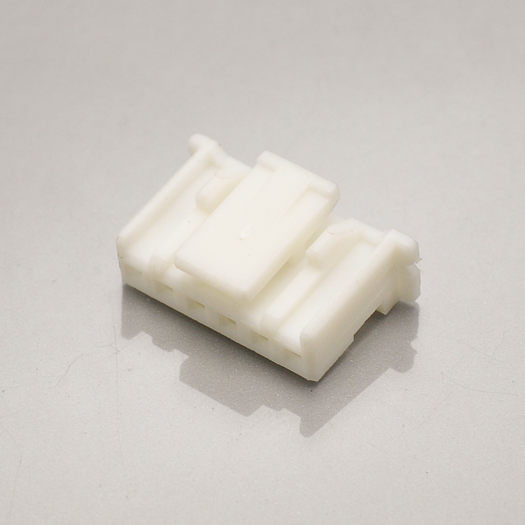
KONNRA KR2014 2.00mm housing, the cross-reference equivalent for the JST PAP housing
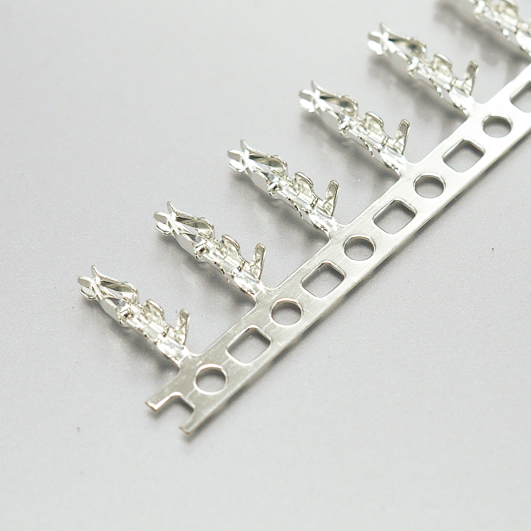
KONNRA KR2014 2.00mm terminal, the cross-reference equivalent for the JST SPHD contact
The four board-side options, in the order the JST prefixes map to them:
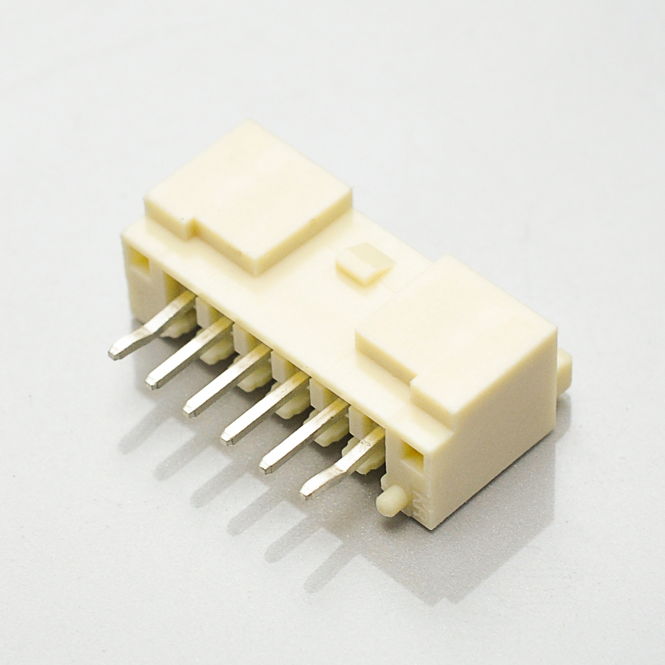
KONNRA KR2014 DIP straight wafer, the cross-reference for the JST PASK top-entry through-hole header
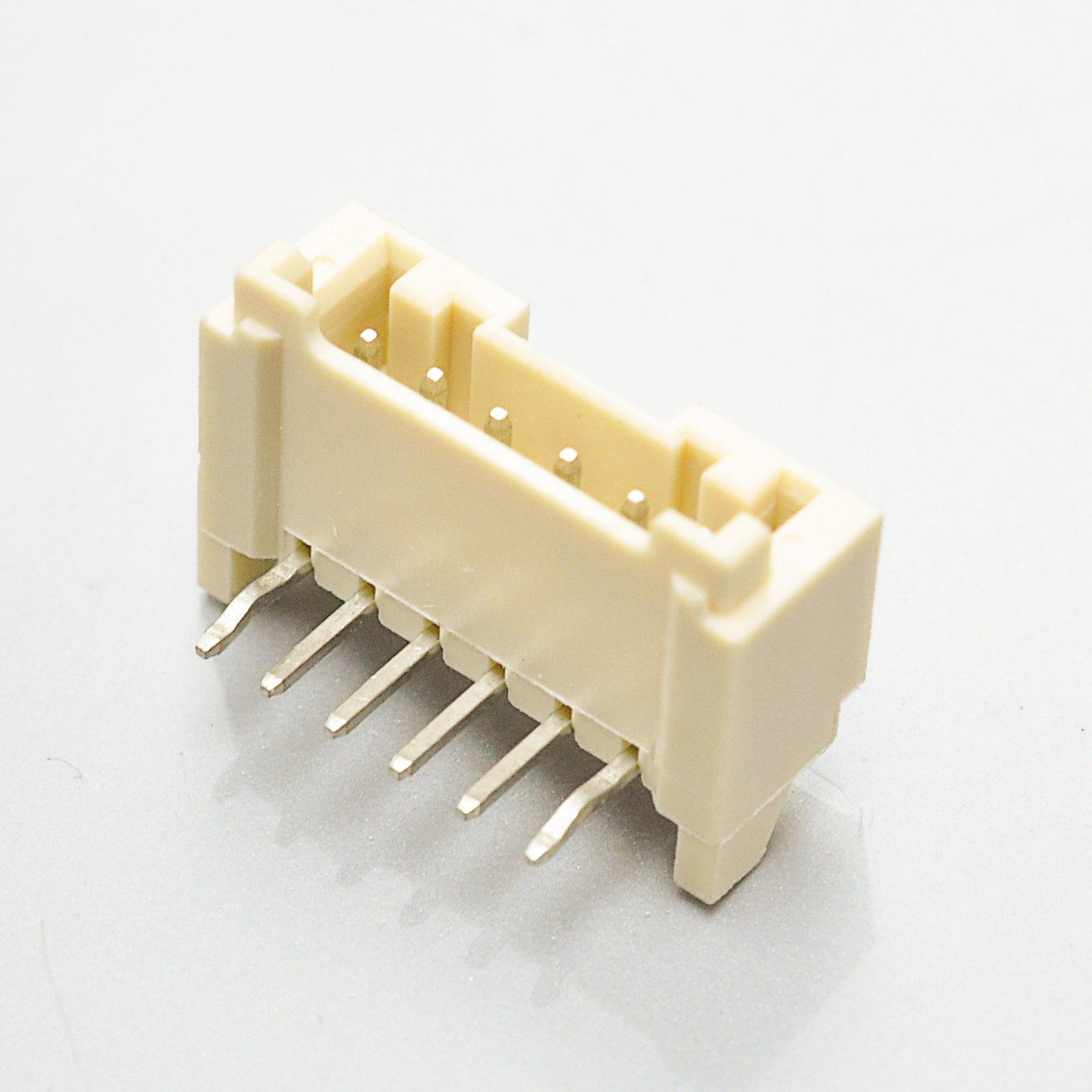
KONNRA KR2014 DIP right angle wafer, the cross-reference for the JST PASK side-entry through-hole header
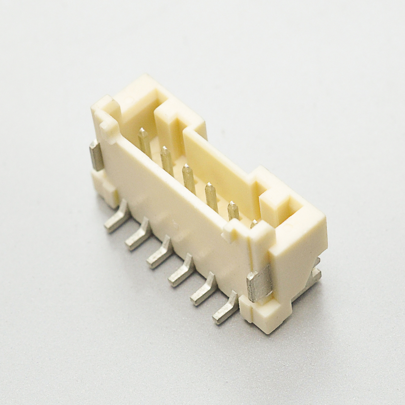
KONNRA KR2014 SMT straight wafer, the cross-reference for the JST PASS top-entry surface-mount header
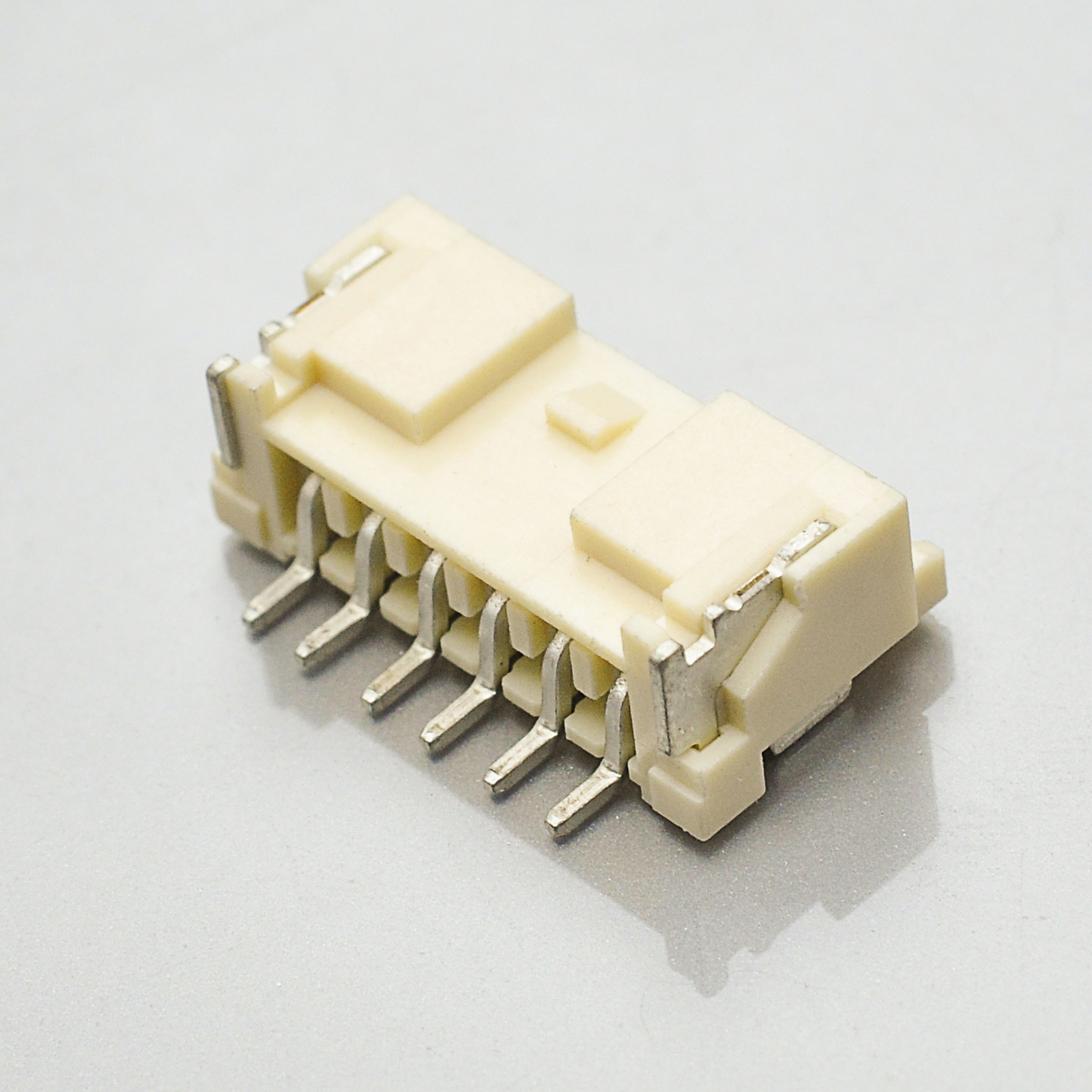
KONNRA KR2014 SMT right angle wafer, the cross-reference for the JST PASS side-entry surface-mount header
Where the KR2014 sits in the 2.00mm class
Two positioning facts are worth knowing, because this catalogue contains several series that look similar from the part number alone.
Within KONNRA’s 2.00mm pitch category, the Series filter enumerates nineteen codes. KR2014 is the JST PA entry among them. Note that the series positioned against JST’s PAL — the wire-to-wire member of the same JST family — is a separate KONNRA series (KR2022), not the KR2014. So the two halves of the JST PA family map onto two different KONNRA series, and the KR2014 covers only the wire-to-board half.
That has a direct consequence for a mixed harness: if you are replacing a design that uses a PA connector at one end and a PAL connector at the other, you need two KONNRA series, not one, and the two will have different published ratings just as the JST originals do.
And the “PA” string is used loosely across the catalogue. Naming a requirement as “2.0mm PA-style” narrows it far less than it sounds — the JST family alone spans three rating sets, two housing architectures and a wire-to-wire branch. Quote the prefix, not the family name, and the comparison resolves in one step.
Cross-reference checklist: ten things to verify before you commit
Work through these in order. The first three decide whether the rest applies.
- Identify the JST variant before anything else. PAP is 250V; PARP and PMS are 100V; PAL is 100V and only −25°C to +85°C. A 250V design that migrates to a retainer-compatible housing is a 100V design, and the difference is invisible from the part number.
- Check for 22 AWG and stop if you find it. The KR2014 covers AWG #24–#28. JST’s 3A rating sits at #22, which this series does not offer, and no KR2014 terminal crimps it. A 22 AWG design has no equivalent here.
- Re-check your contact-resistance budget. JST’s standard PA is 10mΩ initial / 20mΩ after test; the KR2014 is 20mΩ initial / 40mΩ after test. Both figures are published, so this is a straight doubling. Immaterial at 3A; decisive on signal circuits.
- Confirm the circuit count, including whether you need 16. JST’s PAP housing and PASK header run to 16; the KR2014 stops at 15. But JST’s PASS SMT table skips 14, which the KR2014 does cover. The ranges are not nested.
- Settle the wafer base resin. The specification permits PA9T or LCP; every other document names only PA9T. Ask which will be supplied before qualification if either is unacceptable.
- Check whether you need gold at the board interface. Gold is available on the DIP wafer contact but not on the SMT wafer contact, which is matte-tin only. The four wafer pages show tin on all four and will not tell you this.
- Decide whether you need a retainer. JST offers three retainer versions and a separate retainer-compatible housing; the KR2014 documents none. If a retainer is part of your design intent, this is a range gap rather than a specification difference.
- Quote the terminal by its full published number and confirm it. The KR2014 terminal part number carries a 2005 prefix (
T20050P***01A) while every other component in the series carries 2014. Either it is a shared part or it is a transcription error — the documents do not say which. - Check the wire’s insulation diameter, not just its gauge. The KR2014’s insulation window is 0.90–1.40mm against JST’s 0.76–1.50mm. A wire that fits the original may miss at either end of this range.
- Measure the temperature rise at 3A on your actual gauge. The specification’s acceptance limit is 30°C max at rated current. Because the KR2014 reaches 3A on 24 AWG where JST reaches it on 22 AWG, the same current is flowing through less copper — this is the measurement to make on a first article, not an assumption to carry over.
Frequently asked questions
What is the KONNRA KR2014 a replacement for?
The JST PA 2.0 family, specifically its wire-to-board members: the PAP housing, the PASK through-hole headers and the PASS surface-mount headers. It is not a replacement for PAL, the wire-to-wire member of the same JST family, which maps to a different KONNRA series.
Why does “JST PA 2.0” have three different voltage ratings?
Because the family contains three variants with separate specification blocks in the catalogue. The standard PA is 250V AC/DC; the retainer-compatible PA is 100V AC/DC; PAL is 100V AC/DC. They share a 3A current rating and a common mating interface but not a voltage rating, so the variant has to be named before a rating can be quoted.
Can the KR2014 replace a design using AWG #22 wire?
No. The KR2014’s applicable wire range is AWG #24 to #28, and #22 is not a documented option — there is no 22 AWG row in the crimp table. JST’s 3A rating is specified at #22, and JST uses a separate contact (SPHD-001T-P0.5, #26–#22) for that end of its range. The KR2014’s single terminal corresponds to JST’s SPHD-002T-P0.5 branch (#28–#24) and has no equivalent for the other.
Is the 3A rating the same on both parts?
Both documents state 3A, but they specify it at different wire gauges — JST at AWG #22, KONNRA at 24 AWG. The same current through a thinner conductor means higher current density and more self-heating, so the governing check is the specification’s 30°C maximum temperature rise measured at 3A on your own wire. Treat the identical headline figure as a starting point rather than a conclusion.
Why is the contact resistance higher than the original?
20mΩ max initially against JST’s 10mΩ max, and 40mΩ against 20mΩ after environmental testing — a consistent doubling at both points. Both are published figures measured on the same dry-circuit basis, so this is a real difference in the contact system rather than a difference in how the two manufacturers test. It is irrelevant at 3A and significant on low-level signal circuits.
Does the KR2014 come with a retainer?
No. The documentation describes a safety locking device in the housing but no retainer, and JST’s PA family offers three retainer versions plus a separate retainer-compatible housing variant with its own contact. If a retainer is part of your design, that part of the family is out of scope for this series.
What is the difference between PASK and PASS?
PASK is the through-hole (DIP) header — JST publishes it with B**B-PASK for top entry and S**B-PASK for side entry, running 2 to 16 circuits. PASS is the surface-mount header — BM**B-PASS for top entry and SM**B-PASS for side entry, running 2 to 15 circuits with 14 absent from the catalogue table. The KR2014 covers both mounting technologies.
Which wafer do I need for a right angle board connection?
The right angle KONNRA wafer, which maps to JST’s side entry part: S**B-PASK for through-hole or SM**B-PASS for surface-mount. Straight maps to top entry (B**B-PASK / BM**B-PASS). Note that the KONNRA wafer part numbers split their suffix by mounting technology — PA for DIP, RA for SMT — not by orientation, so the suffix will not tell you which angle you have.
Is gold plating available on the KR2014?
Yes on the terminal (tin or gold over nickel) and on the DIP wafer contact (matte-tin or gold over nickel). Not on the SMT wafer contact, which is matte-tin only. If your design requires a gold board interface, it has to use the DIP wafer — and the four wafer component pages show tin on all four, so they will not tell you this.
What material is the wafer made of?
The specification states PA9T or LCP, UL94 V-0. The product page and the four wafer component pages state PA9T / Nylon 9T only. Because the controlling document leaves the choice open, confirm which resin applies before qualification. The housing is a different material — PA66, UL94 V-0, and white.
How many mating cycles does the KR2014 take?
30 cycles, per specification section 7.1, at no more than 10 cycles per minute, with a post-test contact-resistance limit of 40mΩ max. The force table also publishes the withdrawal force after 30 cycles, which is 0.05 kgf lower than the initial value at every circuit count.
Why does the DIP straight wafer page link to a KR2022 drawing?
It is a wrong link on that component page — the DIP Straight Wafer page’s “Series Drawing” button points at KR2022-series-drawing.pdf, a different connector series. The other five component pages link to the correct KR2014-Series-Drawing.pdf. Re-pull any KR2014 straight-DIP drawing from the product page rather than from the component page.
Why do the component pages give three different wire sizes?
They disagree. The housing page says 20#–24#, the terminal page and all four wafer pages say 24#, and the specification says 24#–28#. The specification is the controlling document and the one to use. The housing page’s 20 AWG figure is unsupported by any terminal in the series — there is no 20 AWG crimp row and the terminal’s own range starts at #24.
Does the KR2014 carry UL and LV 214?
All six component pages list UL E482542 / LV 214 under an “Industry Standard” field. No rated voltage is attached to either listing, which is the gap worth closing if your design depends on an agency-recognised voltage — the JST family’s own voltage ratings run from 100V to 250V depending on variant.
Start your cross-reference check
If you are holding a JST PA part number, two facts decide most of the comparison, and both are answerable in minutes.
- Send the housing prefix and the contact part number. PAP means 250V; PARP or PMS means 100V; SPAL means you are in the wire-to-wire branch where the temperature range is only −25°C to +85°C. The prefix settles the rating question faster than any datasheet search.
- Send your wire gauge and insulation diameter. If you are on 22 AWG, the KR2014 is not the part and the conversation ends there. If you are on 24 AWG or finer, check the insulation diameter against 0.90–1.40mm rather than trusting the AWG stamp.
Then ask the two questions the documents cannot answer: which base resin will actually be supplied (PA9T or LCP), and what voltage the UL E482542 listing covers.
The cross-referenced components are the Housing (H201401**0101A, replacing the JST PAP housing), the Terminal (T20050P***01A — confirm this number with the supplier, replacing JST’s SPHD-002T-P0.5 branch), and four wafers replacing the two JST header families: DIP Straight and DIP Right Angle wafers for PASK, SMT Straight and SMT Right Angle wafers for PASS. All are 2.00mm pitch, single row, 2 to 15 circuits, 3A at 24 AWG, 250V AC/DC, −40°C to +105°C, listed to UL E482542 / LV 214, and RoHS compliant.
- View the KONNRA KR2014 PA 2.0 wire-to-board connector series
- Download the KR2014 product specification (PS-KR2014-01)
- Download the KR2014 series drawing
- Send an enquiry to KONNRA
Sources and method
Every figure in this article comes from a manufacturer document and is cited so it can be checked. Where a figure could not be obtained, it is listed as not published rather than estimated.
JST primary document:
- PA FAMILY SERIES / PA・PAF・PAL CONNECTORS catalogue —
jst-mfg.com/product/pdf/eng/ePA-F.pdf. Source of: the three separate specification blocks and their ratings — PA standard type (3A at AWG #22, 250V AC/DC, −40°C to +105°C, contact resistance 10mΩ initial / 20mΩ after test, 1,000MΩ min, 800VAC for one minute, AWG #28–#22, insulation O.D. φ0.76–1.5mm); PA retainer-compatible type (100V AC/DC, contact resistance 15mΩ / 25mΩ, AWG #26–#22, insulation φ0.9–1.5mm, PC board thickness 1.6mm); and PAL (100V AC/DC, −25°C to +85°C, contact resistance 15mΩ/25mΩ, AWG #28–#22, insulation φ0.9–1.5mm, panel thickness 0.5–2.0mm). Also the contact tables forSPHD-002T-P0.5andSPHD-001T-P0.5(8,000 per reel),SPA-001T-P0.5and the PAL contacts (10,000 per reel), all copper alloy tin-plated; the PAP housing table for 2 to 16 circuits with its A and B dimensions and 1,000 per bag; the PARP and PMS retainer-compatible housing tables; the through-hole header tables (B**B-PASK,B**B-PASK-1,S**B-PASK-2,PAFYK,BH**B-PASK,BE**B-PASK) for 2 to 16 circuits with Post: copper alloy tin-plated, Base housing: PBT (GF); the SMT header table (BM**B-PASS,SM**B-PASS) for 2 to 15 circuits with 14 absent, Base housing: PA (Heat Resistance), Reinforcement: copper alloy tin-plated; the secure locking mechanism and keyed housing structure; the three retainer versions; and RoHS2 compliance
KONNRA primary documents:
- Product specification PS-KR2014-01, Rev A1, issued 2022/2/26, 7 pages —
konnra.com/wp-content/uploads/2023/09/PS-KR2014-01.pdf. Source of: the part-number table including the terminal numberT20050P***01A, the materials and plating assignment by component including PA9T or LCP and the Matte-Tin/Gold split between DIP and SMT wafer contacts, the ratings (3A at 24 AWG, 250V, −40 to +105°C, AWG #24–#28, insulation 0.90–1.40mm), sections 5.0 to 7.0 with all eleven environmental and process tests, the uniform 40mΩ post-conditioning limit and the 100MΩ post-humidity insulation resistance, the crimp table, section 6.2–6.4 force figures including the 1.5 kgf terminal retention and the “Checked” field left blank in section 10, both temperature profiles in section 9.0, and the section 8.0 insertion and withdrawal force table for 2 to 15 circuits - Product page and the six component pages: housing, terminal, DIP right angle wafer, DIP straight wafer, SMT right angle wafer, SMT straight wafer. Source of: the three conflicting wire ranges (
20#-24#on the housing page,24#on the terminal and wafer pages,#24~#28on the product page), the housing page’s 10mΩ contact resistance, the six variants of the “Compatible” field, UL E482542 / LV 214, and the DIP straight wafer page’s link toKR2022-series-drawing.pdf - Package specification
Package-spec_KR2014_2024.10.9.pdf— published, 564KB, graphics-only - Series drawing
KR2014-Series-Drawing.pdf— published at 2.0MB; the content is graphics rather than text and could not be extracted, so no figure in this article is quoted from it - 2.00mm pitch category
Method notes:
The two force laws are derived from the specification’s section 8.0 table and are stated as derived. Both relations reproduce all fourteen published values exactly at every circuit count, and the 0.05 kgf loss is a row-by-row subtraction — all fourteen differences are identical rather than approximated. The constant 15× retention ratio is a consequence of the two published per-contact figures (0.10 withdrawal against 1.5 retention) and is presented as arithmetic on published numbers rather than as a tested result.
The “three specifications in one family” finding is a direct reading of three separate ratings blocks printed in JST’s own catalogue, not an inference from part numbers. The variant-to-prefix mapping (PAP / PARP / PMS / PAL) follows the housing and contact tables in that same document.
The three component-page contradictions are direct comparisons of strings published on KONNRA’s own pages, as is the misdirected drawing link. The statement that the wafer cross-reference mappings are semantically correct was verified by checking each KONNRA wafer against the corresponding JST prefix in JST’s header tables — straight against top entry, right angle against side entry, through-hole against PASK and surface-mount against PASS.
Disclosure: this article replaces an earlier, shorter page at the same address. The earlier page did not contain the variant-rating analysis, the wire-gauge comparison against JST’s two-contact arrangement, the force-table derivation, the environmental programme, or the component-page contradictions set out above.
Corrections are welcome and will be made. If a figure here disagrees with the current revision of a manufacturer document, the manufacturer document is right and this article should be corrected against it.