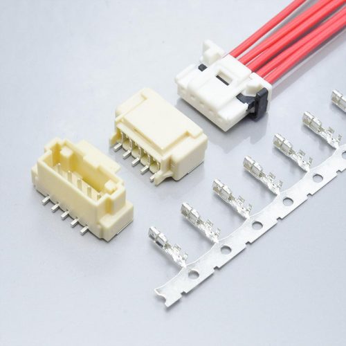
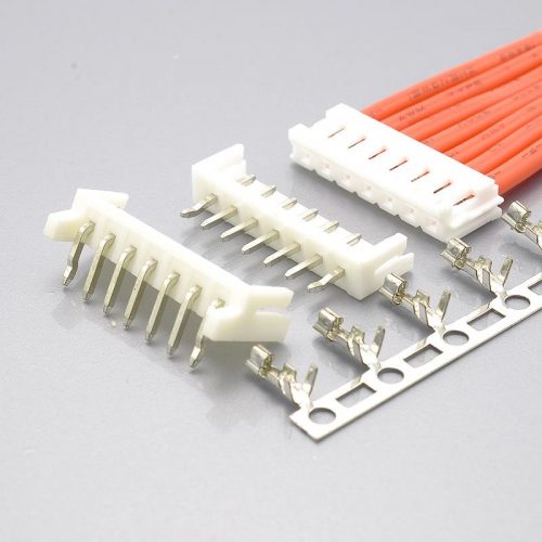
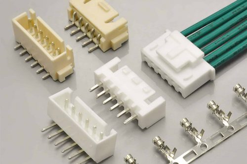
Quick answer: JST SAN is a 2.0mm pitch board-in crimp connector — it has no wafer or header, and the housing itself is soldered to the board. It measures 6.0mm in mounting height and 3.25mm in width, takes AWG #30 to #24 wire with φ0.9–1.3mm insulation, and is rated 2A AC/DC at AWG #24 and 250V AC/DC over −25°C to +85°C, with 800V AC for one minute of withstanding voltage and 1,000MΩ minimum insulation resistance. The KONNRA KR2003 is the cross-reference equivalent. It matches the original’s 250V, 800V withstanding voltage, 1,000MΩ insulation resistance and board-in architecture exactly, and its housing dimensions match JST’s for every circuit count from 2 to 9 — but it widens the temperature range to −40°C/+105°C, and its wire range stops at AWG #28, which is inside JST’s range but leaves AWG #30 uncovered.
There is a second thing worth knowing before anything else, and it is a naming problem rather than a specification problem.
KONNRA publishes this part under the name “KR2003 Equivalent To JST SAN SJN 2.0” — naming both JST series. Those two JST series are not the same connector. SAN is a 2A part with a 2-to-15 circuit range covering every position count. SJN is a 3A part with a 2-to-11 circuit range that skips position 5 entirely. They differ on current, on wire range, on contact material, on housing material and on circuit availability. KONNRA’s own package drawings call this product “SAN2.0”, which is the accurate name — and this guide explains why the distinction matters to anyone reading a datasheet quickly.
Every figure below is traceable to a source listed in the final section. Where a number is not published anywhere we could verify, we say so rather than filling the gap.
At a glance — JST SAN vs the KONNRA KR2003
| Parameter | JST SAN | KONNRA KR2003 | Status |
|---|---|---|---|
| Pitch | 2.0mm | 2.00mm | Match |
| Architecture | Board-in, no wafer | Board-in, wafer: none | Match |
| Mounting height / width | 6.0mm / 3.25mm | not stated | — |
| Circuits | 2 to 15 (all counts) | 2 to 16 (published) | Differs at 16 |
| Rated voltage | 250V AC/DC | 250V AC/DC | Match |
| Rated current | 2A AC/DC (AWG #24) | 2A (24AWG) AC/DC | Match |
| Temperature range | −25°C to +85°C | −40°C to +105°C | Differs |
| Insulation resistance | 1,000MΩ min | 1,000MΩ min | Match |
| Withstanding voltage | 800V AC / 1 minute | 800V AC / minute | Match |
| Applicable wire | AWG #30 to #24 | AWG #24 to #28 | Differs |
| Insulation O.D. | φ0.9–1.3mm | 1.4mm max | Differs |
| Applicable PCB thickness | Type A contact: 1.2mm, 1.6mm · Type K contact: 1.6mm | not stated | See below |
| Contact resistance | not published | 20mΩ max | KONNRA only |
| Terminal material | Copper alloy, tin-plated | Brass, tin plated over nickel | Differs |
| Housing material | PA, yellow | PA66, UL94 V-0, white | Differs |
| Contact types | Two: Type A and Type K (by PCB thickness) | Two: 90° and 180° (by exit direction) | Different axis |
| Durability | not published | 30 cycles | KONNRA only |
| Temperature rise | not published | 30°C max | KONNRA only |
| Mating force table | not published | not published | Neither |
| UL | refer to JST’s registered-standards list | E482542 | KONNRA publishes a number |
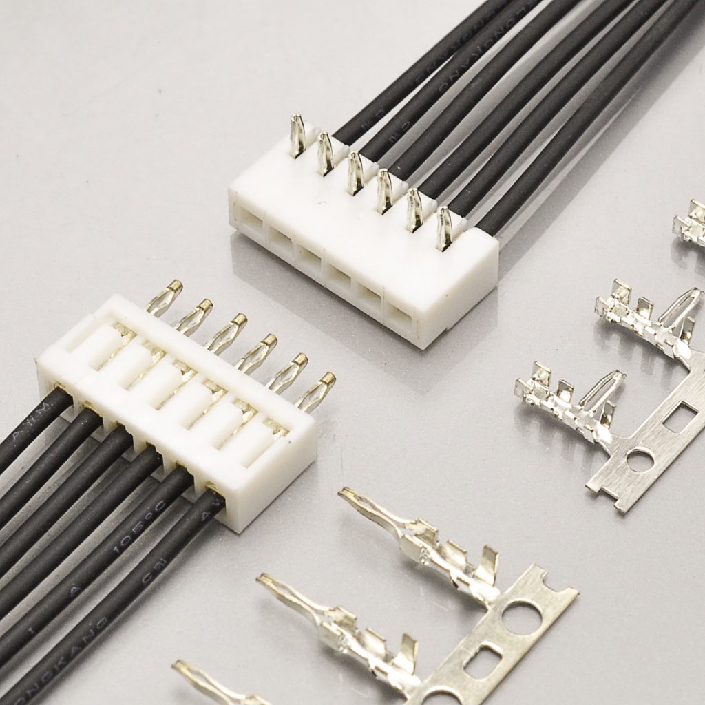
KR2003 — KONNRA’s JST SAN 2.0 board-in equivalent
Three rows in that table decide most design conversations: the temperature range, the wire range, and the PCB thickness. Take them in that order.
What “board-in” means, and why this series has no header to buy
Almost every 2.0mm connector an engineer has met is wire-to-board: a wafer or header solders to the board, a housing crimps onto the wire, and the two mate. The SAN is not that.
On a board-in connector, the housing carries the solder tails. There is no wafer. The housing is placed onto the board and soldered in place, and the crimped terminals are inserted into it from above — the same motion as inserting terminals into a wire-to-board housing, except the housing is now a permanent part of the assembly.
JST describes the SAN as “a multi-circuit board-in connector that increases mounting density on boards and streamlines operations”, and lists six features that all follow from that decision:
- Compact design
- Easy to attach contacts
- Secure mounting on circuit board
- Easy harness processing
- Supports two types of PCB thicknesses
- Two types of contacts
KONNRA’s specification confirms the same architecture from the other side. Its part-number table lists housing and terminal — and then the third row, which is the defining line of the whole series:
| Item | Production part number |
|---|---|
| Housing | H2003R1**0101A · H2003V1**0101A |
| Terminal | T2003RBT0101D · T2003VBT0101A |
| Wafer | None |
Wafer: None. There is no header to buy, no header to place, and no header footprint to reserve.
What it buys you
- One part to place instead of two. No wafer placement step, no separate reflow pass for a header, and no alignment between a header and a housing.
- Board area is the connector’s own footprint. There is no surrounding keep-out for a mating latch or a header shroud. JST leads with exactly this: “increases mounting density on boards.”
- Fewer interfaces. One set of solder joints instead of a solder joint plus a plug-and-receptacle contact pair.
What it costs you
- The connector is not serviceable independently of the board. If the housing is damaged, the repair is a board repair, not a connector swap.
- The wire cannot be disconnected from the board by unplugging a mating pair on the board side — the disconnection point is the terminal-to-housing interface, and repeatedly inserting and withdrawing crimped terminals is not the same operation as mating and unmating two connector halves.
- Your PCB thickness becomes a connector parameter. JST specifies it directly for the SAN, and specifies it differently depending on which contact you choose. A board outside those values needs review before the connector is designed in.
That third point is the one that catches people, because a wire-to-board connector rarely constrains board thickness. On a board-in connector the solder tail length is fixed, so the board has to sit inside the range the tail was designed for — and on this series, the contact type and the board thickness are linked (see the section on Type A and Type K below).
SAN and SJN are two different connectors, and the difference is 50% of the current rating
This is the first thing to resolve on this part, because the naming invites exactly the wrong conclusion.
KONNRA publishes the KR2003 under the title “KR2003 Equivalent To JST SAN SJN 2.0 Alternatives connector” — naming both series as though they were one. They are not. Side by side, as each manufacturer publishes them:
| Parameter | JST SAN | JST SJN |
|---|---|---|
| Description | 2.0mm Wire-to-Board, board-in crimp | 2.0mm board-in crimp |
| Orientation | vertical entry | side entry |
| Mounting height | 6.0mm (width 3.25mm) | 2.8mm (thickness 4.9mm) |
| Current rating | 2A AC/DC (AWG #24) | 3A AC, DC (AWG #22) |
| Voltage rating | 250V AC/DC | 250V AC, DC |
| Temperature range | −25°C to +85°C | −25°C to +85°C |
| Insulation resistance | 1,000MΩ min | 1,000MΩ min |
| Withstanding voltage | 800V AC / 1 minute | 800 VAC / minute |
| Applicable wire | AWG #30 to #24 | AWG #28 to #22 |
| Insulation O.D. | φ0.9 to 1.3mm | 1.1–1.4mm (-001PT) · 0.9–1.4mm (-002PT) |
| Applicable PCB thickness | Type A: 1.2mm, 1.6mm · Type K: 1.6mm | 1.2 to 1.6mm |
| Circuits | 2 to 15 — every count | 2 to 4, and 6 to 11 — no 5-position |
| Housing material | PA, yellow | PA 66, UL94V-0, natural (white) |
| Contact material | Copper alloy, tin-plated | Brass, tin-plated (reflow treatment) |
| Contact part numbers | SAN-002T-0.8A · SAN-002T-0.8K |
SJN-001PT-0.9 · SJN-002PT-0.9 |
| Housing part numbers | 2P-SAN … 15P-SAN |
02P-SJN … 11P-SJN |
| Recognised standard | refer to JST’s registered-standards list | Recognized E60389 |
Four differences in that table will change a design decision, and one of them is easy to miss entirely.
The current rating differs by 50%. SAN is a 2A part; SJN is a 3A part, rated at the larger AWG #22 wire. A designer who reads “SAN SJN” and needs 3A has arrived at the wrong connector. The KR2003 publishes 2A, which matches SAN and not SJN.
SJN has no 5-position. Its housing table runs 02, 03, 04, 06, 07, 08, 09, 10, 11 — the 5-circuit part simply does not exist, and the JST datasheet states the range explicitly as “No. of circuits: 2 to 4, 6 to 11”. SAN covers every count from 2 to 15. So if a 5-position requirement is anywhere in your BOM, SAN is the family that can serve it and SJN is not — and this is the kind of gap that is invisible in a headline circuit range.
The wire ranges overlap only in the middle. SAN takes #30–#24; SJN takes #28–#22. They share only #28, #26 and #24. So “2.0mm board-in JST” tells you almost nothing about which wire your harness can use until you know which of the two families you are holding.
And the contact materials are not the same. SAN’s contacts are copper alloy; SJN’s are brass. That is a difference in the spring material at the heart of the connector, not a plating detail.
Where the KR2003 actually sits
Laid against both, the KR2003’s published specification is unambiguous:
| Evidence | Points to |
|---|---|
| Current 2A | SAN (SJN is 3A) |
| Voltage 250V | both (identical) |
| Wire AWG #24–28 | inside SAN’s #30–24; overlaps SJN’s #28–22 |
| Housing dimensions | SAN (match at every count — see the dimension section) |
| Terminal material brass | SJN (SAN is copper alloy) |
| Housing material PA66 UL94 V-0 | SJN (SAN is PA, yellow) |
| Circuits 2–15, every count | SAN (SJN has no 5-position) |
Electrically and dimensionally it is a SAN part; two of its material choices follow SJN. And KONNRA’s own drawings resolve the naming: the package specification is titled “SAN2.0 Housing Packing” and its terminal packing drawings are titled “SAN2.0 180°Terminal Packing” and “SAN2.0 90°Terminal Packing”, with drawing numbers in the 2003H01-A-P / 2003TV101-A-P / 2003TR01-D-P series.
So: if you need SAN, this is the right cross-reference. If you need SJN — and specifically its 3A rating, its AWG #22 capability, or its 2.8mm side-entry profile — ask us before assuming anything, because the published name on the page does not distinguish between the two.
The wire range: AWG #30 is where the cross-reference stops
JST publishes the SAN’s wire range as AWG #30 to AWG #24, with insulation O.D. from φ0.9mm to φ1.3mm, and it offers a single contact operating across that whole span (SAN-002T-0.8A and SAN-002T-0.8K both list #30–24 with insulation 0.9–1.3mm).
KONNRA publishes:
Applicable wire: AWG 24# ~ 28#, Insulation O.D. 1.40 mm MAX
Both the product specification §4.0 and the component pages give the same range — and, unusually for this catalogue, the product page and the Overview prose agree with the specification too. There is no page-versus-specification contradiction on this series.
Lay the two ranges against each other:
| Gauge | JST SAN | KONNRA KR2003 |
|---|---|---|
| AWG #30 | ✅ SAN-002T-0.8A / -0.8K |
❌ not covered |
| AWG #28 | ✅ | ✅ |
| AWG #26 | ✅ | ✅ |
| AWG #24 | ✅ | ✅ |
AWG #30 is inside JST’s range and outside the KR2003’s. The KR2003 covers a three-gauge subset (#24, #26, #28) of the SAN’s four-gauge range.
That gap is smaller than the ones we have documented on other series, and it is a clean subset rather than an offset — but it is still a real limit, and on a board-in connector small wire is common, because the whole reason to choose this architecture is dense mounting in a compact product.
And the insulation window is stated differently
JST gives a window: φ0.9mm to φ1.3mm. KONNRA gives a ceiling: 1.4mm maximum.
Two consequences, and they run in opposite directions:
- A wire with 1.35mm insulation is outside JST’s SAN window and inside KONNRA’s published limit. The KR2003 claims a larger upper bound than the original accepts. Physically that may be fine — but it is a specification difference, not a match, and if your design was qualified against SAN’s 1.3mm ceiling, moving to a 1.4mm wire is a change that needs its own justification.
- A wire below 0.9mm insulation has no published JST SAN equivalent — and the KR2003 states no lower bound at all, so it neither confirms nor denies one.
The practical rule is the same one that applies to every crimp connector on this list. The insulation crimp height is set against the insulation diameter, and 1.4mm is the ceiling KONNRA publishes for the KR2003’s terminal. Measure your wire’s insulation rather than reading the diameter off a catalogue page, and compare the measurement against 0.9–1.3mm (SAN) as well as against 1.4mm max (KR2003) — the narrower window is the one that governs a substitution.
The temperature range: JST says −25°C to +85°C, KONNRA says −40°C to +105°C
Both JST board-in 2.0mm series publish −25°C to +85°C, with the explicit qualification that the range “includ[es] temperature rise in applying electrical current.”
- JST SAN: −25°C to +85°C
- JST SJN: −25°C to +85°C
- KONNRA KR2003: −40°C to +105°C
That is 20°C wider at the cold end and 20°C wider at the hot end. And unlike the situation we documented on another 2.00mm series in this catalogue, all four KONNRA sources agree — the product specification §4.0, the product page’s General Specification table, the product page’s Overview prose and the component pages all state −40°C to +105°C. There is no internal contradiction to resolve here; there is simply a cross-reference part claiming a wider range than the original publishes.
And the claim is backed by KONNRA’s own test programme. The same specification publishes the tests behind the rating:
| Test | Condition | Requirement |
|---|---|---|
| Heat resistance (§7.5) | 105 ± 2°C, 96 hours (EIA-364-17B) | No damage; contact resistance 40mΩ max |
| Cold resistance (§7.6) | −40 ± 2°C, 96 hours (EIA-364-59) | No damage; contact resistance 40mΩ max |
| Thermal shock (§7.8) | −40°C 30 min → room temp 5 min → +105°C 30 min → room temp 5 min = 1 cycle, 5 cycles (EIA-364-32B) | No damage; contact resistance 40mΩ max |
The rated extremes are the tested extremes, held for 96 hours each and cycled five times between them.
How to use that difference
If you are replacing a SAN in an existing product designed to JST’s range, your design basis is 85°C at the top and −25°C at the bottom. The KR2003’s range is a potential improvement, not a requirement, and switching to it does not invalidate the existing thermal margins.
If your application needs to operate below −25°C or above +85°C, the original SAN is outside its published operating range and the KR2003’s range becomes the relevant document. JST’s −25°C floor is notably shallow — it is the same floor JST publishes on the SJN and on several other series — so a cold-soak or outdoor-winter requirement will rule the original out on paper. This is one of the cases where a cross-reference may genuinely be better than the original rather than merely equivalent.
And if you need the number to stand up in a qualification file, ask for the raw report behind §7.5, §7.6 and §7.8 rather than the summary table. A specification that names its test standards (EIA-364-17B, −59, −32B) is a specification whose underlying data can be requested.
One caution that applies to both parts. The +105°C figure is the connector’s own capability. It says nothing about the wire insulation you crimp into it — and on this series the insulation is already constrained to a 0.9–1.3mm window by the crimp. A high-temperature requirement has to be satisfied by the wire as well as by the housing.
PCB thickness: the parameter JST publishes and the cross-reference does not
On a board-in connector, board thickness is not a board parameter — it is a connector parameter. The solder tail length is fixed, so the board has to sit inside the range the tail was designed for.
JST publishes it for the SAN, and links it to the contact type:
| Contact type | Applicable PC board thickness |
|---|---|
Type A (SAN-002T-0.8A) |
1.2mm and 1.6mm |
Type K (SAN-002T-0.8K) |
1.6mm |
Read that carefully, because it explains why JST lists “Supports two types of PCB thicknesses” and “Two types of contacts” as separate features. The two contact types exist to serve different board thicknesses, and the Type A contact covers two of them while the Type K covers only one. Choosing a contact is therefore partly a board decision, not only a harness decision.
For comparison, JST’s SJN specifies 1.2 to 1.6mm with no contact distinction.
KONNRA’s KR2003 specification does not publish an applicable PCB thickness. Not in §4.0, not in the component pages, not on the product page. We checked the specification, the component pages, the product page and the package specification; none of them states one.
That is the most consequential gap on this series for a board-in design, and it is more significant than the AWG #30 gap, because:
- A wrong board thickness is a mechanical failure, not a marginal electrical derating. A tail designed for 1.6mm in a 1.2mm board leaves less solder fillet than intended; the reverse leaves the housing standing off the board.
- It is invisible on a specification table. Nothing in the ratings or the environmental data hints at it.
- It is a question with a fast answer — our engineering team can confirm the applicable thickness for the specific KR2003 part number you intend to use, in writing, against the current drawing.
And note the second half of the problem: the contact-type axis does not map. JST varies its contact by board thickness (Type A / Type K); KONNRA varies its contact by wire exit direction (90° / 180°). Those are different axes, and there is no published row that tells you which KR2003 housing to buy for a 1.2mm board. If your board is 1.2mm and you are replacing a SAN Type A contact, that is the first question to ask — not the last.
The ratings that match exactly
Four parameters — including the two hardest to match on a 2.0mm board-in part — agree between JST’s SAN datasheet and KONNRA’s KR2003 specification, at the same qualified conditions:
Rated voltage: 250V AC/DC on both. Identical figures, same qualifier. And note how unusual a 250V rating is in this pitch: it is well above the 125V and 100V values that dominate the 2.00mm class, and it is one of the reasons this family exists alongside cheaper 2.0mm options.
Rated current: 2A AC/DC at AWG #24 on both. JST writes “Current rating: 2 A AC/DC (AWG #24)”; KONNRA writes “Rated Current (Max.) 2A(24AWG) AC/DC”. Same figure, same gauge, same qualifier.
Insulation resistance: 1,000MΩ minimum on both. JST states it plainly; KONNRA specifies it by method — 500V DC for one minute between adjacent contacts, to EIA-364-21B.
Withstanding voltage: 800V AC for one minute on both. JST writes “There shall be no breakdown or flashover while applying 800 VAC for one minute.” KONNRA writes “Apply 800V AC for 1 minute between adjacent terminal or ground” with the acceptance criteria “No Breakdown and Flashover”, to EIA-364-20A.
Both of the last two are worth pausing on. A 250V rated voltage alongside an 800V AC proof voltage is a 3.2× relationship, which is a sensible margin for a connector in this class — and the two manufacturers land on identical figures for both. A cross-reference that matches a proof voltage exactly is a cross-reference whose dielectric construction is genuinely the same, not merely described the same way. On this series there is no need for the “request written confirmation of the higher figure” step that we have flagged on other parts.
And the one parameter KONNRA publishes alone
Contact resistance: 20mΩ max, specified by KONNRA and not published on JST’s SAN datasheet. (JST’s SAN specification set covers current, voltage, temperature, insulation resistance, withstanding voltage, conductor size, insulation O.D. and PCB thickness — contact resistance is not among them.) The KR2003’s figure is measured by dry circuit at 20mV / 100mA between the A and B regions of the mated pair, to EIA-364-23C, with a 40mΩ max allowance after the environmental tests.
So the two documents are complementary rather than redundant, and the split is clean:
- JST publishes the board-side geometry — mounting height, width, PCB thickness per contact type, hole pitch tolerance, and the layout notes.
- KONNRA publishes the electrical and environmental qualification — contact resistance, the durability figure, temperature rise, and the full vibration / shock / thermal / humidity / salt-spray programme with its EIA standards named.
You need both documents. A complete qualification file for a KR2003 substitution should contain JST’s board layout and board-thickness data (because KONNRA does not publish a thickness), plus KONNRA’s environmental programme and crimp specification (because JST does not publish them for the SAN).
The housing dimensions: an exact match up to 9 circuits, then 0.20mm
This is the most reassuring part of the comparison, and it is checkable to the last decimal.
KONNRA publishes a full housing dimension table for both the 180° and 90° versions. JST publishes one for the SAN housing. Laid side by side for the 180° (vertical) version:
| Circuits | JST 2P-SAN A / B |
KONNRA H2003V1NN0101A A / B |
Difference in B |
|---|---|---|---|
| 2 | 2.0 / 5.2 | 2.00 / 5.20 | — |
| 3 | 4.0 / 7.2 | 4.00 / 7.20 | — |
| 4 | 6.0 / 9.2 | 6.00 / 9.20 | — |
| 5 | 8.0 / 11.2 | 8.00 / 11.20 | — |
| 6 | 10.0 / 13.2 | 10.00 / 13.20 | — |
| 7 | 12.0 / 15.2 | 12.00 / 15.20 | — |
| 8 | 14.0 / 17.2 | 14.00 / 17.20 | — |
| 9 | 16.0 / 19.2 | 16.00 / 19.20 | — |
| 10 | 18.0 / 21.2 | 18.00 / 21.40 | +0.20 |
| 11 | 20.0 / 23.2 | 20.00 / 23.40 | +0.20 |
| 12 | 22.0 / 25.2 | 22.00 / 25.40 | +0.20 |
| 13 | 24.0 / 27.2 | 24.00 / 27.40 | +0.20 |
| 14 | 26.0 / 29.2 | 26.00 / 29.40 | +0.20 |
| 15 | 28.0 / 31.2 | 28.00 / 31.40 | +0.20 |
| 16 | not published | 30.00 / 33.40 | no JST counterpart |
Three things come out of that table, and they are all precise enough to put in a design review.
The A dimension — the one that governs the pitch progression and the footprint — matches JST exactly at every circuit count from 2 to 15. It advances by exactly 2.00mm per circuit on both sides, with no exceptions.
The B dimension matches exactly from 2 through 9 circuits, then is consistently 0.20mm larger from 10 circuits upward. The 0.20mm is precisely the stated general tolerance on KONNRA’s drawings (X.XX ± 0.20), so this sits inside tolerance and is almost certainly a difference in what each drawing chose to nominate as the nominal at the longer lengths rather than a design change. But if your enclosure, a neighbouring component or a wire-routing channel is dimensioned tightly against a 21.2mm B on a 10-position part, you are 0.20mm longer than you planned — and that is worth confirming rather than assuming.
And the 16-position housing has no JST counterpart at all. JST’s SAN housing table stops at 15P-SAN. KONNRA publishes H2003V1160101A (16 positions) and H2003R1**160101A. So the 16-position market is KONNRA’s own extension and should be qualified as such — it is not a cross-reference at all, because there is nothing on the JST side to cross-reference against.
The 90° housing table publishes only the A dimension, and it runs from 2.00mm at 2 positions to 30.00mm at 16 positions in 2.00mm steps — the same progression as the 180° version, which is consistent with the two orientations sharing a footprint and differing only in which way the housing body extends.
Two part numbers in the 90° housing table do not follow the series’ own rule
The KR2003 housing numbering follows a clear convention: undefined + undefined or undefined (vertical or right angle) + a three-digit circuit code + undefined. So the 5-position 180° housing is H2003V1050101A, the 10-position is H2003V1100101A, and the 15-position is H2003V1150101A.
In the published 90° housing table, the two highest circuit counts break that pattern:
| Circuits | Published 90° part number | What the rule predicts |
|---|---|---|
| 2 | H2003R1020101A |
✓ |
| … | … | ✓ |
| 14 | H2003R1140101A |
✓ |
| 15 | H2003R150101A | H2003R1150101A |
| 16 | H2003R160101A | H2003R1160101A |
The 15- and 16-position entries are each one digit short, and they do not match the 180° housing’s numbering for the same circuit counts (H2003V1150101A and H2003V1160101A, which follow the rule correctly).
We are not going to assert which string is the correct orderable part number — that is a question for the supplier, and it is one we will answer in writing. What can be stated is the observation: two part numbers in that table are inconsistent with the series’ own numbering convention and with the equivalent entries in the 180° table. If you are ordering a 15- or 16-position 90° KR2003 housing, confirm the part number rather than transcribing it — a one-digit difference in a connector part number is invisible once the parts are out of the bag.
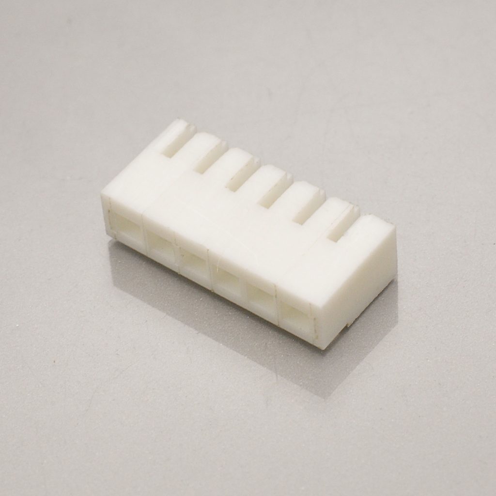
KR2003 180° housing

KR2003 90° housing
The contact axis: JST varies by board thickness, KONNRA varies by exit direction
This is the distinction that most often causes a wrong order on this series, because both manufacturers offer two contact types — and they are not the same two types.
JST SAN offers two contacts, differentiated by which PCB thickness they serve:
| JST contact | Type | Applicable wire | Insulation O.D. | Qty/reel | PCB thickness |
|---|---|---|---|---|---|
SAN-002T-0.8A |
Type A | AWG #30–24 (0.05–0.22mm²) | 0.9–1.3mm | 14,000 | 1.2mm and 1.6mm |
SAN-002T-0.8K |
Type K | AWG #30–24 (0.05–0.22mm²) | 0.9–1.3mm | 14,000 | 1.6mm |
Both cover the same wire range and the same insulation window. The only published difference is the board thickness the contact is designed for. Material and finish: copper alloy, tin-plated on both. JST’s model-number allocation reads SAN-002T-0.8A, where the 002 segment is the applicable wire range, T is the tin-plated finish, and the trailing A / K is the type.
KONNRA offers two terminals and two housings, differentiated by wire exit direction:
| KONNRA terminal | Orientation | Crimp spec in §6.3 / §6.4 |
|---|---|---|
T2003VBT0101A |
180° (vertical) | §6.4 |
T2003RBT0101D |
90° (right angle) | §6.3 |
And the corresponding housings: H2003V1**0101A (180°) and H2003R1**0101A (90°).
So the axes are different, and there is no published mapping. A customer holding a SAN Type K contact — specified for a 1.6mm board — cannot look up “which KR2003 terminal” from any published table, because the KR2003’s two terminals encode exit direction, not board thickness. That is the question to ask before ordering, and it is the second half of the PCB-thickness gap identified above.
And the two KR2003 terminals do not share a crimp specification
Here is something worth knowing even if you never touch a JST part. KONNRA publishes separate crimp tables for the 90° and 180° terminals — and they differ on two parameters:
| Crimp parameter | 24 AWG | 26 AWG | 28 AWG |
|---|---|---|---|
| Conductor crimp width (both terminals) | 1.30 ± 0.10 | 1.30 ± 0.10 | 1.30 ± 0.10 |
| Conductor crimp height (both terminals) | 0.75 ± 0.05 | 0.70 ± 0.05 | 0.60 ± 0.05 |
| Insulation crimp width (both terminals) | 1.50 ± 0.10 | 1.50 ± 0.10 | 1.50 ± 0.10 |
| Insulation crimp height — 90° | 1.50 ± 0.10 | 1.40 ± 0.10 | 1.20 ± 0.10 |
| Insulation crimp height — 180° | 1.55 ± 0.10 | 1.45 ± 0.10 | 1.40 ± 0.10 |
| Crimp strength (both terminals) | 3.63 kgf min | 2.27 kgf min | 1.36 kgf min |
| Stripping length — 90° | 2.4–2.8mm | ||
| Stripping length — 180° | 1.5–2.0mm |
The conductor crimp — width, height and strength — is identical between the two terminals. The insulation crimp and the stripping length are not.
Two consequences, and both are production-floor issues rather than design-document issues:
A line running both terminals cannot share a stripping setup. The 90° terminal needs 2.4–2.8mm of strip; the 180° terminal needs 1.5–2.0mm. Those windows do not overlap — the 180° terminal’s maximum is below the 90° terminal’s minimum. A single stripping length setting will be wrong for one of them.
A crimp-height check written for one terminal will misjudge the other. The insulation crimp height targets differ by 0.05mm at 24 and 26 AWG and by 0.20mm at 28 AWG, and every window is only ±0.10mm wide. At 28 AWG the two targets (1.20mm and 1.40mm) sit exactly at each other’s window edges — so a 28 AWG insulation crimp correct for the 180° terminal is out of tolerance for the 90° terminal, and vice versa.
And the conductor crimp height window is ±0.05mm at every gauge, stepping down 0.05mm per wire size — 0.75, 0.70, 0.60. A 0.10mm wide window on a sub-millimetre target is a tight process, and it is why the applicator setup is worth verifying by measurement rather than by eye.
Crimp strength falls by a factor of 2.7 across the wire range — 3.63 kgf at AWG #24 down to 1.36 kgf at #28. If your harness mixes gauges, your pull-test acceptance criterion differs per circuit, and a single pass/fail figure will either pass bad crimps at 24 AWG or reject good ones at 28 AWG.

KR2003 180° terminal

KR2003 90° terminal
How to identify which board-in 2.0mm connector you are holding
The 2.00mm pitch class contains well over a dozen series in KONNRA’s own index, and the board-in subset contains at least three from JST alone. Work through these in order — the first two questions do most of the work.
1. Is there a wafer? Look at the board. If you can see a separate header soldered down with a housing that plugs onto it, this is a wire-to-board connector, not a board-in one. If the housing itself is soldered to the board and the crimped terminals push in from above, it is board-in — and in the 2.00mm pitch class that narrows the field sharply.
2. Measure the height, and the entry direction. This is the decisive question between the two JST board-in families:
- 6.0mm mounting height, vertical entry, 3.25mm width → SAN
- 2.8mm mounting height, side entry, 4.9mm thickness → SJN
The SJN is a dramatically lower-profile part because it enters from the side. If you are looking at a low, side-entering board-in connector in 2.0mm pitch, it is not SAN.
3. Count the positions, and check for the gap. SJN has no 5-position connector. Its published range is 2 to 4 and 6 to 11. SAN covers every count from 2 to 15. So a 5-position board-in 2.0mm housing is SAN (or a cross-reference to it) and cannot be SJN — a useful positive identification, and one you can make by counting rather than by measuring.
4. Look at the housing colour. JST’s SAN housing is documented as PA, yellow. JST’s SJN housing is PA 66, UL94V-0, natural (white). Colour is not a specification, but on a populated board it is the fastest way to tell two otherwise similar families apart — and it is the kind of thing that survives into a photograph you can send someone.
5. Check the contact’s base metal if you can, or read the contact part number. SAN contacts are copper alloy; SJN contacts are brass. Both are tin-plated, so the finish will not distinguish them visually. The part numbers will: SAN-002T-0.8A and SAN-002T-0.8K for SAN, SJN-001PT-0.9 and SJN-002PT-0.9 for SJN. KONNRA’s equivalents are T2003VBT0101A (180°) and T2003RBT0101D (90°).
6. If the wire is loose, measure the insulation diameter. SAN accepts φ0.9–1.3mm; SJN accepts 0.9–1.4mm on one contact and 1.1–1.4mm on the other. Only the 0.9–1.3mm band is common to both, so a wire measuring inside that band tells you nothing — but a wire measuring 1.35mm rules SAN out.
7. And if the board is accessible, measure its thickness. SAN is specified for 1.2mm and 1.6mm with the Type A contact, and 1.6mm with the Type K contact. SJN is specified for 1.2 to 1.6mm. A board outside those ranges is evidence that either this is not the connector or that it was used outside its specification. Either finding is worth knowing.
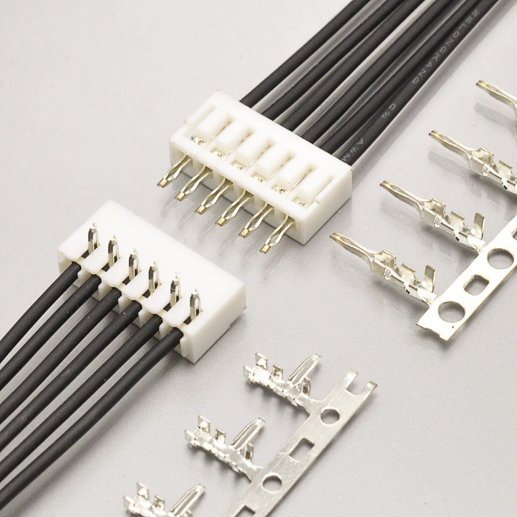
KR2003 — 2.00mm pitch board-in connector
Where SAN sits in the 2.00mm class
KONNRA’s own 2.00mm index lists more than fifteen series spanning a 2.5× range in current and a 2.5× range in voltage. The table below uses KONNRA’s published cross-reference positioning, so the entries are the supplier’s own:
| KONNRA series | Cross-references to | Architecture | Current | Voltage | Circuits |
|---|---|---|---|---|---|
| KR2003 | JST SAN 2.0 | Board-in | 2A | 250V | 2–16 |
| KR2000 | Molex MicroBlade mx2.0 | DIP wire-to-board | 2A | 125V | 2–15 |
| KR2001 | JST PH 2.0 | Wire-to-board | 2A | 100V | 2–16 |
| KR2002 | IL-S | Wire-to-board | 2A | 100V | 2–16 |
| KR2004 | Yeonho YH200 PH 2.0 | Wire-to-board with lock | 2A | 250V | 2–16 |
| KR2005 | JST PHD 2.0 | Wire-to-board, 2 rows | 3A | 250V | 2*2–2*20 |
| KR2007 | Molex mx2.0 | Wire-to-wire | 2A | 125V | 2–16 |
| KR2009 | Hirose DF3 | Wire-to-board | 3A | 250V | 2–15 |
| KR2014 | JST PA 2.0 | Wire-to-board | 3A | 250V | 2–15 |
| KR2017 | Molex DuraClik mx2.0 | Wire-to-board | 3A | 125V | 2–14 |
| KR2022 | JST PAL 2.0 | Wire-to-board | 3A | 250V | 2–14 |
| KR2023 | JST ULH 2.0 | Wire-to-board, TPA | 5A | 100V | 2–10 |
Four observations worth carrying into a design review.
Board-in is rare in this class, and that is the whole reason to consider this series. KONNRA’s own Board-In Connector category lists only five products across all pitches. In the 2.00mm pitch, the KR2003 is the board-in option — everything else in the table needs a wafer, and a wafer needs board area, a placement step and a footprint. If your requirement is board-in, most of this table is eliminated before you compare a single electrical parameter.
The KR2003 sits in the high-voltage half of the class. At 250V it joins the KR2004, KR2005, KR2009, KR2014 and KR2022 — and sits well above the 100V entries (KR2001, KR2002, KR2023) and the 125V entries (KR2000, KR2007, KR2017). Since board-in connectors are typically used for internal signal and small power distribution rather than for high-voltage work, that 250V rating is generous for the architecture — and it comes directly from JST’s SAN datasheet rather than being a cross-reference upgrade.
Two entries in this table are named “PH 2.0”, and one of them is a lock. The KR2001 cross-references JST PH 2.0 at 100V; the KR2004 cross-references Yeonho YH200 PH 2.0 at 250V with a lock. Same pitch, same 2–16 circuits, same 2A, different originals, different voltage, different retention. Note also that KR2004 carries the same 250V rating as the KR2003 — so a customer who needs both a high voltage rating and a lock has an option in this catalogue, and the two are easy to confuse by name.
And note where the wire-to-wire entry sits. The KR2007 is the only wire-to-wire part in the table. If a requirement says “2.00mm, and it must be wire-to-wire”, architecture decides it before ratings do — SAN is not a candidate.
The environmental qualification, and the UL number
On the environmental side the two documents do not overlap at all, and this time it is not a case of each side covering half — it is a case of one side publishing a programme and the other publishing nothing in this area.
JST’s SAN datasheet does not publish a durability figure, a temperature-rise figure, or any vibration, shock, thermal, humidity or salt-spray requirement. Its specification set covers current, voltage, temperature range, insulation resistance, withstanding voltage, conductor size, insulation O.D., PCB thickness, and the standards reference — and stops there.
KONNRA’s KR2003 specification publishes the full programme:
| Item | Condition | Requirement |
|---|---|---|
| Durability (§7.1) | 30 cycles, at no more than 10 cycles/minute (EIA-364-09C) | Contact resistance 40mΩ max |
| Temperature rise (§7.2) | Carrying rated current load (EIA-364-70B) | 30°C max |
| Vibration (§7.3) | 1.5mm P-P, 10→55→10 Hz in 1 minute, 2 hours per axis in X, Y and Z (EIA-364-28B) | No damage; contact resistance 40mΩ max; discontinuity 1 microsecond max |
| Mechanical shock (§7.4) | 490 m/s² (50g), 3 strokes in each of 6 directions (EIA-364-27B) | No damage; 40mΩ max; discontinuity 1 microsecond max |
| Heat resistance (§7.5) | 105 ± 2°C, 96 hours (EIA-364-17B) | No damage; 40mΩ max |
| Cold resistance (§7.6) | −40 ± 2°C, 96 hours (EIA-364-59) | No damage; 40mΩ max |
| Humidity (§7.7) | 40 ± 2°C, 90–95% RH, 96 hours (EIA-364-31B) | No damage; 40mΩ max; must meet §5.3; insulation resistance 100MΩ min |
| Thermal shock (§7.8) | −40°C 30 min → RT 5 min → +105°C 30 min → RT 5 min, 5 cycles (EIA-364-32B) | No damage; 40mΩ max |
| Salt spray (§7.9) | 24 hours, 35 ± 2°C, 5 ± 1% NaCl (EIA-364-26B) | No damage; 40mΩ max |
| Solderability (§7.10) | 245 ± 5°C, 3 ± 0.5 seconds (EIA-364-52) | ≥95% of immersed area free of voids and pin holes |
| Solder heat resistance (§7.11) | Terminal tip in solder at 250°C max, 3–5 seconds, 0.8mm from tip (EIA-364-71B) | No damage |
Read the two contact-resistance columns together, because they tell you what the environmental work costs. The part is specified at 20mΩ max when new (§5.1) and 40mΩ max after every one of the exposures above. That relaxation is normal, it is specified rather than hidden, and it means a used connector is allowed twice the contact resistance of a new one — which matters if your design carries any margin on contact resistance at all.
And read the humidity line specifically, because a relaxed figure is easy to misread. KONNRA’s §7.7 requires 40mΩ max contact resistance, no dielectric breakdown, and 100MΩ minimum insulation resistance after 96 hours at 90–95% RH. That 100MΩ is a post-humidity allowance, not the part’s rating — which remains 1,000MΩ minimum under §5.2 and matches JST. Do not carry 100MΩ into a specification as the insulation resistance.
Two things neither side publishes for this series, and they are worth being explicit about because they are both normally available on comparable parts:
- There is no insertion or withdrawal force table. The KR2003’s specification goes from the crimp sections straight to the environmental section — its §6.0 covers terminal insertion force (0.5 kgf / 4.9N max), terminal/housing retention (1.0 kgf / 9.8N min) and the two crimp tables, and then §7.0 is environmental, §8.0 is the remark. There is no per-circuit mating force table, and JST’s SAN datasheet does not publish one either. So on this series the mating force is undocumented on both sides — a contrast with other series in this catalogue where one or both manufacturers publish a full 2-to-16 circuit table.
- Neither side publishes a soldering profile. JST’s SAN datasheet carries no process data beyond the board layout. KONNRA’s KR2003 specification has solderability (§7.10) and solder heat resistance (§7.11) but no §9.0 profile section of the kind that appears on its other board-in and SMT series. So the process window has to come from your own profiling run rather than from either document. The two solder limits that are published — 245 ± 5°C for 3 ± 0.5 seconds for solderability, and 250°C maximum for 3–5 seconds for heat resistance — bracket the process, and both sit comfortably inside a standard lead-free profile.
The UL number, and what it does and does not mean
KONNRA’s KR2003 component pages publish an industry standard entry:
Industry Standard — UL — E482542
This is worth noting for two reasons, and clarifying for a third.
It is a published UL file number for the KR2003 itself — which is more than several other series in this catalogue provide, where no UL or CSA number appears anywhere in KONNRA’s documentation. If your qualification file requires a recognised component, that number is available for this part.
It is KONNRA’s own recognition, not a transfer of JST’s. A UL file number appearing on a cross-reference part means that part has been evaluated and listed under that file — it does not mean the part inherits, or is covered by, the original manufacturer’s recognition. JST’s own recognitions are separate: the SJN datasheet states Recognized E60389, and the SAN datasheet directs customers to JST’s “List of Registered Overseas Standards” rather than stating a number on the page.
And JST adds a warning that applies to any cross-reference on a certified product:
“Specifications registered to overseas standards may differ from the general specifications listed above.”
If your product is submitted under a registration, the registered specification governs — and it may not be the datasheet figure you are comparing against. On a cross-reference part, that means there are potentially three relevant specifications: your registered one, JST’s general one, and KONNRA’s. Where they differ, the registered one wins.
Board layout and process
Three JST layout notes apply to the SAN, and two of them cause rework when ignored.
The layout is drawn from the soldering side. JST’s SAN datasheet says: “The PC board layout figure shown is viewed from the soldering side.” Board-in footprints are frequently drawn this way and frequently read the other way. Confirm the mirroring before you release a footprint, because the error only surfaces once the connectors arrive.
The hole pitch tolerance is ±0.05mm and does not accumulate. JST states: “Tolerance for the PCB hole pitch shall be ± 0.05 and shall not accumulate.” Non-cumulative is the important word — the error does not build up across 15 positions, so the tolerance applies per pitch rather than to the total length of a 15-position footprint.
The hole dimensions are a guideline, not a specification. JST states: “Hole dimensions differ depending on the type of PCB and PCB drilling method.” And for boards using a hard material composed of fiberglass cloth, JST’s PH datasheet advises considering a larger hole diameter. If you are releasing a board-in footprint for production, that is a conversation with the supplier rather than a dimension to copy from a PDF — and on a board-in part it matters more than usual, because the housing is the connector: a solder defect at a housing tail is a board rework, not a header replacement.
And the board thickness assumption has to be made explicitly — see the section above. JST links the contact type to the board thickness (Type A: 1.2mm and 1.6mm; Type K: 1.6mm), and KONNRA publishes no equivalent figure for the KR2003. That is the one design input on this series that cannot currently be read off a published document, and it is the first thing we would confirm in writing for a specific part number.
Packaging
KONNRA’s package specification for the KR2003 covers both the housing and the terminals:
- Housings: 1,000 pieces per bag, listed for circuit counts 2 through 15
- Terminals: 10,000 pieces per reel
- Cartons in three sizes (L460×W460×H510mm, L500×W500×H305mm, L580×W580×H320mm), selected by order quantity
- The specification is marked RoHS compliant
Note what the housing packing table stops at: 15 circuits. KONNRA’s product page and Overview both describe the series as 2 to 16 circuits, and the housing dimension tables do include a 16-position part — but the only place KONNRA enumerates this series’ circuit counts in a packing document stops at 15, and JST’s SAN housing table also stops at 15. So the 16-position part is KONNRA’s own extension, published in the dimension tables and the component pages, and it has no counterpart on the JST side to cross-reference against. If you need 16 positions, treat it as a new part to qualify rather than as a substitution.
Cross-reference checklist: ten things to verify before you commit
Work through these in order. Each one corresponds to a specific difference or open question identified in this guide.
| # | Check | Why |
|---|---|---|
| 1 | Confirm you need SAN and not SJN | Both JST series are 2.0mm board-in and the KR2003’s page names both. SAN is 2A; SJN is 3A at AWG #22. The KR2003 publishes 2A, which matches SAN. |
| 2 | Check whether your position count exists in the original | JST SAN covers 2–15, every count. JST SJN skips 5 and stops at 11. The KR2003 publishes 2–16 — and 16 has no JST counterpart at all. |
| 3 | Confirm your wire gauge is inside AWG #24–28 | The KR2003’s published range stops at #28, so AWG #30 is uncovered even though it is inside JST’s #30–24 range. |
| 4 | Measure your wire’s insulation O.D. | JST specifies a window of φ0.9–1.3mm; the KR2003 publishes a 1.4mm maximum. A 1.35mm wire is outside the original’s window and inside the cross-reference’s limit. |
| 5 | Establish the applicable PCB thickness — this is the open item | JST links it to the contact type (Type A: 1.2mm and 1.6mm · Type K: 1.6mm). KONNRA publishes no board thickness for the KR2003. Ask before you lay out the board. |
| 6 | Resolve the contact axis, which does not map | JST varies its contact by board thickness; KONNRA varies by wire exit direction (90° / 180°). There is no published row converting one to the other. |
| 7 | Set the crimp per terminal, not per series | The 90° and 180° KR2003 terminals have different insulation crimp heights and non-overlapping stripping windows (2.4–2.8mm vs 1.5–2.0mm). One setup cannot serve both. |
| 8 | Decide which temperature range you are designing to | JST publishes −25°C to +85°C; the KR2003 publishes −40°C to +105°C, backed by its own 96-hour heat, cold and thermal-shock tests. |
| 9 | Confirm the part number for 15- and 16-position 90° housings | Two entries in the published 90° housing table — H2003R150101A and H2003R160101A — are one digit short of the series’ own numbering rule and of the equivalent 180° part numbers. |
| 10 | If your product is certified, cite the registered specification | The KR2003 carries UL E482542 — KONNRA’s own recognition, not a transfer of JST’s. And JST warns that “specifications registered to overseas standards may differ from the general specifications.” |
Items 1, 5 and 6 are the three that produce a wrong part or a blocked design. Item 1 is a family-selection error that the published page name actively invites; item 5 is a missing specification you cannot read off any document; and item 6 is an axis mismatch between two published sets of options.
Frequently asked questions from procurement and engineering
Is the KR2003 a drop-in replacement for JST SAN? On the electrical core it matches closely: 250V, 2A at AWG #24, 1,000MΩ insulation resistance and 800V AC/minute withstanding voltage all agree with JST’s published figures at matched conditions, and the A dimension of the housing matches exactly at every circuit count from 2 to 15. The B dimension matches through 9 circuits and is 0.20mm larger from 10 upward — inside the drawing’s own ±0.20 tolerance, but worth confirming if your layout is tight. It differs on the wire range (#24–28 against #30–24) and on the temperature range, and it does not publish an applicable PCB thickness, which JST does. Treat it as a documented cross-reference to be qualified, not as a pin-compatible drop-in — and send us your board thickness and footprint and we will confirm both.
Is it a SAN or an SJN equivalent? SAN. The page title names both series, but the evidence points to SAN on every decisive parameter: 2A (SJN is 3A), housing dimensions matching SAN exactly, and all position counts from 2 to 15 (SJN skips 5 and stops at 11). KONNRA’s own package drawings call the product “SAN2.0”, which is the accurate name. Two of its material choices — a brass terminal and a PA66 UL94 V-0 housing — follow SJN rather than SAN, but those do not change the electrical or mechanical identity of the part.
What is the actual current rating? 2A AC/DC at AWG #24. JST writes “2 A AC/DC (AWG #24)” and KONNRA writes “2A(24AWG) AC/DC” — the same figure at the same qualified gauge. Note that the rating is qualified by the wire on both documents, and the KR2003’s wire range stops at AWG #28, so the 2A applies at #24 and the capability at smaller gauges is bounded by the conductor.
Does it cover AWG #30? No. The KR2003’s published range is AWG #24 to #28. JST’s SAN takes AWG #30 to #24. So AWG #30 is inside the original’s range and outside the cross-reference’s — a one-gauge gap at the fine end. If your harness uses AWG #30, ask us before designing it in; that is a specific configuration question rather than an assumption to make from the datasheet.
What PCB thickness does it suit? This is the open item on this series. JST specifies the SAN for 1.2mm and 1.6mm with the Type A contact and 1.6mm with the Type K contact. KONNRA’s KR2003 specification does not publish an applicable board thickness — we checked the specification, the product page, the component pages and the package specification. On a board-in connector, where the solder tail length is fixed and the board has to fit it, this is a design input rather than a detail. Send us your board thickness and the part number you intend to use and we will confirm it in writing against the current drawing.
Which contact type do I need — Type A or Type K? On the JST side, that is a board-thickness question: Type A serves 1.2mm and 1.6mm, Type K serves 1.6mm only. Both cover the same wire range (AWG #30–24) and the same insulation window (0.9–1.3mm), so the wire does not decide it — the board does. On the KONNRA side there is no Type A/Type K equivalent; its two terminals are the 180° (T2003VBT0101A) and the 90° (T2003RBT0101D), differentiated by wire exit direction. If you are replacing a Type A or Type K contact, tell us your board thickness and we will identify the matching KR2003 configuration — the two manufacturers’ contact options are not interchangeable by name.
What is the correct temperature range? Both figures are correct for their own part. JST publishes −25°C to +85°C for the SAN, qualified as including temperature rise under load. The KR2003 publishes −40°C to +105°C, and all four KONNRA sources agree — the specification, the product page’s specification table, the page’s Overview prose and the component pages. The KR2003’s range is backed by 105±2°C / 96-hour heat, −40±2°C / 96-hour cold and five-cycle thermal-shock tests. So the cross-reference part claims a range 20°C wider at both ends than the original publishes.
Does it have a lock? No. The SAN is a board-in part with no latch and no mating pair on the board side — the housing is soldered down and the housing-to-board joint is a solder joint. Retention is the terminal’s fit in the housing, specified by KONNRA at 1.0 kgf (9.8N) minimum. If your requirement is written as “positive locking connector”, this architecture does not satisfy it, on either manufacturer’s version of the part.
How many mating cycles does it have, and how much force does mating take? 30 cycles on the KR2003, with contact resistance required to stay at or below 40mΩ afterwards. JST’s SAN datasheet does not publish a durability figure. On mating force: neither manufacturer publishes a per-circuit insertion or withdrawal force table for this series — a contrast with other series in this catalogue where one or both sides publish a full table. What is published are the assembly-side forces: terminal insertion force 0.5 kgf (4.9N) max and terminal/housing retention 1.0 kgf (9.8N) min.
What standards does it carry? The KR2003 carries UL file E482542, published on its component pages — that is KONNRA’s own recognition of its own part, not a transfer of JST’s. JST’s SAN datasheet refers to its “List of Registered Overseas Standards” rather than stating a number; JST’s SJN states Recognized E60389. JST also warns that “specifications registered to overseas standards may differ from the general specifications listed above” — so on a certified product, cite the registered specification.
What are the lead time and MOQ? KONNRA can deliver complete connector set samples within 45 days. Connector production lead time is typically 2–3 weeks, and wiring harness assemblies are quoted separately. Housings are packed 1,000 per bag and terminals 10,000 per reel; MOQ depends on the circuit count and the terminal orientation — send the specific configuration and it will be quoted against the actual part numbers.
What is the difference between the KR2003 and the KR2004? Different originals and different architectures. The KR2003 cross-references JST SAN 2.0 — board-in, no wafer, 2A, 250V, 2–16 circuits. The KR2004 cross-references Yeonho YH200 PH 2.0 — wire-to-board with a lock, 2A, 250V, 2–16 circuits. They share a pitch, a voltage rating and a current rating, and they are completely different connector systems. See our other 2.00mm and adjacent-pitch guides, including the JST PH 2.0 connector guide, the Molex MicroBlade 2.0 connector guide, the Molex CLIK-Mate 1.5 connector guide and the JST SZN 1.5 connector guide.
Start your cross-reference check
Send us the four things below and we will come back with a specific answer rather than a catalogue page — including, if you send the drawing, a footprint comparison against the SAN part you are replacing:
- Your board thickness — the one input we cannot read off a published document for the KR2003, and the first question on a board-in design
- Your wire gauge and measured insulation O.D. — we will check it against the KR2003’s AWG #24–28 range and 1.4mm maximum, and against JST’s 0.9–1.3mm window
- Your position count — and whether it is a count that exists in JST’s SAN range at all (2–15), or 16, which is KONNRA’s own extension
- Which JST contact you are replacing — Type A or Type K — so we can map it to the right KR2003 configuration, since the two manufacturers’ contact axes differ
From that we can confirm the housing and terminal part numbers, the applicable board thickness, the crimp specification, and — where a figure in our published material is thinner than the original’s, such as the wire range — give you a written answer against the controlled specification.
- Request a quote — KR2003 pricing, MOQ and configuration for your circuit count, terminal orientation and wire gauge
- Request a sample — complete connector set samples delivered within 45 days
- Request a board-thickness confirmation — the applicable PCB thickness for your specific KR2003 part number, in writing, against the current drawing
- Request a footprint and contact mapping check — send your SAN drawing or footprint and your board thickness, and we will confirm the A and B dimensions and identify the matching KR2003 contact configuration
- Request the documents — product specification PS-KR2003-01 (PDF), package specification (PDF), 180° housing drawing (PDF), 180° terminal drawing (PDF), and the series drawing (PDF)
- Request a crimp specification sheet — separate conductor and insulation crimp heights, widths and pull-strength requirements for the 90° and 180° terminals across 24, 26 and 28 AWG, including the stripping lengths
- Request a vendor qualification pack — test capability summary, quality documentation and the UL recognition details behind E482542
- Request assembled harnesses — KR2003 board-in assemblies crimped and tested to the specification above
- Submit a drawing for review — we will flag any specification mismatch before you commit tooling
Contact KONNRA Electronics
- Phone: (86)-769-85449875
- Email: info@konnra.com
- Address: No.6 Nanchang South Road, Chijiao, Wangniudun, Dongguan, Guangdong, China
- Contact us
Orderable components: KR2003 180° Housing · KR2003 90° Housing · KR2003 180° Terminal · KR2003 90° Terminal
➡️ Explore the full 2.0mm pitch range · Board-In connector category · JST connector cross-reference: 20+ series
Sources and method
This guide compares the original manufacturer’s published documentation with KONNRA’s own published documentation for the cross-reference part. Where the two disagree — and where KONNRA’s own documents disagree with each other — both figures are shown and the discrepancy is stated rather than resolved by preference.
Original manufacturer (JST):
- JST SAN connector datasheet (
eSAN.pdf), JST product documentation. Used for: the series description (“2.0mm pitch/Wire-to-Board connectors/Board-in Crimp style”, “a multi-circuit board-in connector that increases mounting density on boards and streamlines operations”); pitch 2.0mm, mounting height 6.0mm, width 3.25mm; the feature list including “Supports two types of PCB thicknesses” and “Two types of contacts”; current rating 2A AC/DC (AWG #24); voltage rating 250V AC/DC; temperature range −25°C to +85°C including temperature rise; insulation resistance 1,000MΩ min; withstanding voltage 800 VAC for one minute with no breakdown or flashover; conductor size AWG #30 to #24; insulation O.D. φ0.9mm to φ1.3mm; applicable PC board thickness — Type A contact 1.2mm and 1.6mm, Type K contact 1.6mm; RoHS2 compliance; the standards note directing customers to the “List of Registered Overseas Standards” and the warning that “specifications registered to overseas standards may differ from the general specifications listed above”; the board layout notes (“viewed from the soldering side”, ±0.05 tolerance for the PCB hole pitch, non-cumulative, and the hole-dimension caveat); the contact table (SAN-002T-0.8AType A andSAN-002T-0.8KType K, both AWG #30–24, insulation 0.9–1.3mm, 14,000 per reel, material copper alloy, tin-plated); the model number allocation (SAN-002T-0.8A); the crimping machine table (AP-K2N, MKS-L, APLMK SAN002-08); and the housing table (2P-SANthrough15P-SAN, A 2.0–28.0mm, B 5.2–31.2mm, 1,000 per bag, material PA, yellow). - JST SJN connector datasheet (
eSJN.pdf), JST product documentation. Used for: the series description (“Side entry type board-in connector, with a mounting height of only 2.8 mm and a thickness of 4.9 mm”); the feature list (housing lances, easy mounting onto printed circuit boards); current rating 3A AC, DC (AWG #22); voltage rating 250V AC, DC; temperature range −25°C to +85°C; insulation resistance 1,000MΩ min; withstanding voltage 800 VAC/minute; applicable wire AWG #28 to #22; applicable PC board thickness 1.2 to 1.6mm; the standard Recognized E60389; the board layout notes; the contact table (SJN-001PT-0.9— 0.20–0.33mm², AWG 24–22, insulation 1.1–1.4mm, 15,000/reel;SJN-002PT-0.9— 0.08–0.22mm², AWG 28–24, insulation 0.9–1.4mm, 18,000/reel; material brass, tin-plated (reflow treatment)); the crimping machine tables; the housing table (02P-SJNthrough11P-SJN, skipping 5, A 2.0–20.0mm, B 4.4–22.4mm, material PA 66, UL94V-0, natural (white)) and its explicit circuit-range statement “No. of circuits: 2 to 4, 6 to 11”.
Cross-reference manufacturer (KONNRA) — KR2003 series:
- Product specification PS-KR2003-01, Edition A1, issued and revised 2022/2/26, Engineering Dept., Dongguan Konnra Electronics Co., Ltd, six pages. Used for: §2.0 the part-number table (housings
H2003R1**0101AandH2003V1**0101A; terminalsT2003RBT0101DandT2003VBT0101A; wafer: none); §3.0 materials and surface treatment (PA66, UL94 V-0 housing; brass, tin plated over nickel terminal; wafer rows marked N/A); §4.0 ratings (250V AC/DC, 2A (24AWG) AC/DC, −40°C ~ +105°C, AWG 24#–28# with insulation O.D. 1.40mm max); §5.1 contact resistance 20 milliohms max by dry circuit at 20mV / 100mA to EIA-364-23C; §5.2 insulation resistance 1000 megohms min at 500V DC for one minute to EIA-364-21B; §5.3 dielectric strength 800V AC for one minute to EIA-364-20A; §6.1 terminal insertion force 0.5 kgf (4.9N) max; §6.2 terminal/housing retention 1.0 kgf (9.8N) min; §6.3 the crimp specification for the 90° terminal and §6.4 for the 180° terminal, including the differing insulation crimp heights and the differing stripping lengths (2.4–2.8mm and 1.5–2.0mm respectively) and the crimp strengths (3.63 / 2.27 / 1.36 kgf min); §7.1–7.11 the environmental performance including durability (30 cycles), temperature rise (30°C max), vibration, shock, heat, cold, humidity (40±2°C, 100 megohms min after), thermal shock, salt spray (24 hours), solderability and solder heat resistance; and §8.0 the remark. Note what this specification does not contain: an applicable PCB thickness, a soldering profile section, and a per-circuit insertion/withdrawal force table. - Package specification, drawing number 2003H01-A-P, Rev A1, marked RoHS compliant, titled “SAN2.0 Housing Packing”, with terminal packing drawings 2003TV101-A-P (“SAN2.0 180°Terminal Packing”) and 2003TR01-D-P (“SAN2.0 90°Terminal Packing”). Used for: 1,000 pieces per bag for housings across circuit counts 2 to 15; 10,000 pieces per reel for terminals; the three carton sizes; and the internal product name “SAN2.0”.
- Engineering drawings, KR2003 series: KR2003-Series-Drawing_180-housing.pdf (the 180° housing dimension table,
H2003V1NN0101A, giving the A and B dimensions for 2 to 16 circuits) and KR2003-Series-Drawing_90-housing.pdf (the 90° housing table,H2003R1NN0101A, giving the A dimension for 2 to 16 circuits). The series drawing and the 180° and 90° terminal drawings were not retrievable in text form during this review, so the terminal geometry and the recommended PCB layout could not be transcribed and are not compared here. - KR2003 product page and the four component pages (180° Housing, 90° Housing, 180° Terminal, 90° Terminal). Used for: the page specification table (pitch 2.00mm, circuits 2–16pin, current 2A, voltage 250V; materials; insulation O.D. 1.4mm max; withstanding 800V AC/minute; temperature −40°C to +105°C; contact resistance 20mΩ max; insulation resistance 1000MΩ min; plating tin over nickel); the General Specifaction table; the Overview prose (including the “AWG #24-#28” and “2 to 16 circuits” statements); the Advantages section; the component part names and assembly types (Board In); the per-component feature tables including number of rows 1, number of positions 2P~16P, colour white, material PA66 UL94 V-0, wire size 24#-28# and the industry standard entry UL E482542; the component and document download links; and the image set.
- KONNRA 2.0mm pitch index page and the Board-In Connector category page. Used for the cross-reference positioning of the sibling 2.00mm series (KR2000, KR2001, KR2002, KR2004, KR2005, KR2007, KR2009, KR2014, KR2017, KR2022, KR2023) in the pitch-class comparison table, and for the observation that KONNRA’s Board-In category lists five products across all pitches.
Not published in any source reviewed: an applicable PCB thickness for the KR2003; a soldering profile for either the SAN or the KR2003; a per-circuit insertion/withdrawal force table for either; a durability figure, temperature-rise figure or environmental test programme for the JST SAN; contact resistance for the JST SAN; the terminal geometry and recommended PCB layout for the KR2003 (drawings not retrievable); and a mounting height or width for the KR2003. Two internal inconsistencies are reported rather than resolved: the 90° housing part numbers for 15 and 16 circuits (H2003R150101A and H2003R160101A) are one digit short of the series’ own numbering convention and of the equivalent 180° part numbers, and the 16-position range appears in the dimension tables and component pages while the only document that enumerates the series’ circuit counts for packing purposes stops at 15.
Method note. Figures were taken from controlled or manufacturer-published documents where available. The SAN-versus-SJN distinction was established by comparing both JST datasheets parameter by parameter rather than relying on the series name, which is how the 3A-versus-2A current difference, the absence of a 5-position in SJN, the differing wire ranges and the different contact materials were identified. The wire range was compared gauge by gauge across both manufacturers’ contact tables rather than as a headline range, which is how the AWG #30 gap was identified. The housing dimensions were transcribed and differenced position by position; the A dimension was confirmed identical at every circuit count from 2 to 15 and the B dimension was found identical from 2 to 9 and consistently +0.20mm from 10 to 15, with that 0.20mm noted as equal to the drawings’ own general tolerance band (X.XX ± 0.20). The two crimp tables were compared row by row, which is how the differing insulation crimp heights and the non-overlapping stripping windows were identified; the conductor crimp parameters were confirmed identical between the two terminals. No claim is made about the KR2003’s applicable board thickness, because no published document states one.