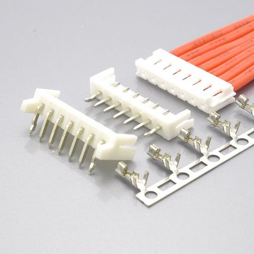
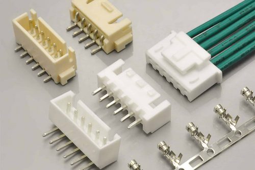
Quick answer: The JST SZN is a 1.5mm pitch board-in crimp connector — it has no wafer, and the housing itself is soldered directly onto the PCB at a mounting height of 4.25mm. JST rates it at 0.7A AC/DC (AWG #26) and 50V AC/DC, over −25°C to +85°C, for AWG #30 to #26 wire. The KONNRA KR1502 is the cross-reference equivalent, and it carries a 1A rating in its published specification. That gap between 0.7A and 1A is the single most important thing to check before you substitute one for the other — this guide explains why it exists and what to do about it.
The JST SZN is one of the least glamorous connectors in the 1.5mm class, and that is roughly the point. It exists to do one job: terminate a small-gauge wire bundle directly onto a printed circuit board with no mating header, no secondary connector half, and no board real estate spent on a separate wafer footprint.
That design choice — board-in, rather than wire-to-board — is what makes this series behave differently from almost everything else engineers compare it against, including the JST ZH that shares its 1.5mm pitch. It is also why the series is more often specified than discussed: there is very little written about it, and the numbers that circulate are frequently borrowed from a neighbouring family.
This guide covers the system as JST documents it, as the KONNRA KR1502 documents it, and — importantly — the places where those two sets of documents do not agree. Every figure below is traceable to a source listed in the final section. Where a number is not published anywhere we could verify, we say so instead of filling the gap.
At a glance — SZN 1.5 and KR1502 side by side
| Parameter | JST SZN (original) | KONNRA KR1502 (cross-reference) | Status |
|---|---|---|---|
| Pitch | 1.5mm | 1.50mm | Match |
| Architecture | Board-in, no wafer | Board-in, wafer: none | Match |
| Mounting height | 4.25mm | not stated | — |
| Thickness | 2.4mm | not stated | — |
| Rated current | 0.7A AC/DC (AWG #26) | 1A (@ 26 AWG) | Differs |
| Rated voltage | 50V AC/DC | 50V (§4.0) / 200V (drawing & page table) | Differs internally |
| Temperature range | −25°C to +85°C | −40°C to +105°C | Differs |
| Withstanding voltage | 500V AC/minute | 500V AC/minute | Match |
| Insulation resistance | 500MΩ min | 500MΩ min | Match |
| Contact resistance | not published in JST’s SZN rating set | 20mΩ max | — |
| Applicable wire | AWG #30 to #26 | AWG #26 to #30 | Match |
| Insulation O.D. | 0.8–1.1mm (002) · 0.7–0.9mm (003) | 1.0mm max | Differs |
| Circuits | 2 to 13 | 2 to 16 | Differs |
| Applicable PCB thickness | 0.6 to 1.2mm | not stated | — |
| Housing material | PA 66, UL94V-0, natural (white) | PA66, UL94 V-0 | Match |
| Terminal material | Phosphor bronze | Phosphor bronze / brass | Differs |
| Terminal finish | Tin-plated (reflow treatment) | Tin plated over nickel | Differs |
| Standards | UL Recognized E60389 · CSA LR20812 | not stated | — |
| RoHS | RoHS2 | RoHS compliant | Match |
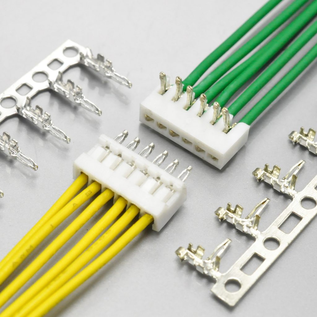
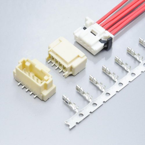
KR1502 series — 1.5mm pitch SZN board-in connector
Three rows in that table are flagged “Differs”, and one of them is flagged twice for a reason that has nothing to do with KONNRA at all. Read the rest of this guide before you treat any of them as a simple substitution decision.
What “board-in” actually means, and why it changes the comparison
Almost every 1.5mm connector an engineer has seen up to this point is wire-to-board: a wafer (header) solders to the board, a housing crimps onto the wire, and the two mate. The SZN is not that.
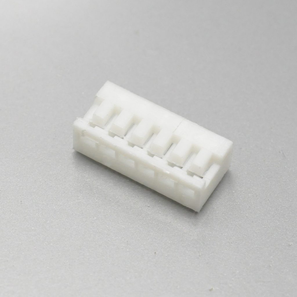
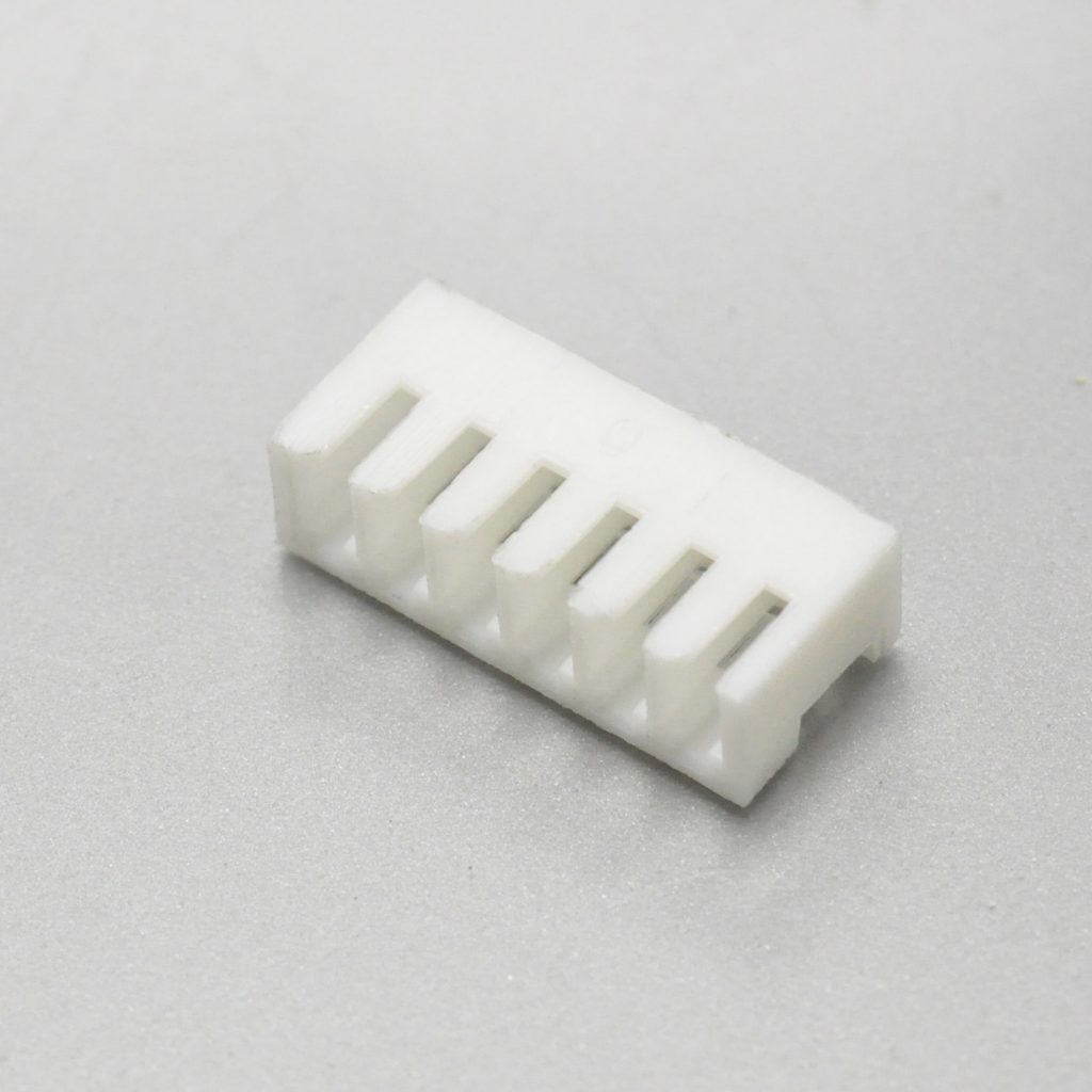
On a board-in connector, the housing carries the solder tails. There is no wafer. The housing is placed onto the board and soldered in place, and the crimped terminals are inserted into it from above — the same way they would be inserted into a wire-to-board housing, except the housing is now a permanent part of the assembly.
The JST datasheet describes the design in one sentence: “This low-profile, board-in connector, with a mounting height of only 4.25 mm and a thickness of 2.4 mm, is soldered directly onto printed circuit boards.” It adds two mechanical details that matter during assembly: “The solder tail of the contact is resilient for easy assembly” and “The housing lances facilitate insertion of contacts.”
The KONNRA specification sheet confirms the same architecture from the other side. Its part-number table is laid out in two columns — item and production part number — and the item column carries three rows. The third one is the one that matters:
| Item | Production part number |
|---|---|
| Housing | H150201**0101A |
| Terminal | T1502VPT010*A · T1502RBT010*A |
| Wafer | None |
(The source document is bilingual, Chinese and English; the table above reproduces the part numbers exactly as printed.)
Wafer: None. That is the defining line of the whole series. There is no header to buy, no header to place, and no header footprint to reserve.
What this buys you
- One part to place instead of two. No wafer placement, no separate reflow step for a header, no alignment between a header and a housing.
- Board area is the connector’s own footprint. There is no surrounding keep-out for a mating header latch.
- Fewer interfaces. One solder joint set instead of a solder joint plus a plug-and-receptacle contact pair.
What it costs you
- The connector is not serviceable independently of the board. If the housing is damaged, the repair is a board repair, not a connector swap.
- The wire harness cannot be disconnected from the board by unplugging a mating pair on the board side — the disconnection point is the terminal-to-housing interface, and repeated insertion and withdrawal of crimped terminals is not the same as mating and unmating two connector halves.
- Your PCB thickness becomes a connector parameter. JST specifies an applicable PCB thickness of 0.6 to 1.2mm for the SZN. A board outside that window needs review before you design the connector in.
That third point is easy to miss, because a wire-to-board connector rarely constrains board thickness. On a board-in connector, the solder tail length is fixed and the board thickness has to sit inside the range the tail was designed for.
The system as JST documents it
JST publishes the SZN as a single 1.5mm pitch board-in crimp series. The full published specification set is short, which is convenient — here it is in its entirety:
| Item | JST published specification |
|---|---|
| Current rating | 0.7A AC/DC (AWG #26) |
| Voltage rating | 50V AC/DC |
| Temperature range | −25°C to +85°C (including temperature rise under current) |
| Insulation resistance | 500MΩ min |
| Applicable wire | AWG #30 to #26 |
| Withstanding voltage | 500V AC/minute |
| Applicable PCB thickness | 0.6 to 1.2mm |
| Standards | UL Recognized E60389 · CSA Certified LR20812 |
| Compliance | RoHS2 |
Two details in that table are worth pausing on before we get to the contradictions.
The current rating is qualified by wire gauge, not stated as a single number. JST writes “0.7A AC/DC (AWG #26)” — the rating is given at the largest wire the series accepts. This is normal practice, but it means the 0.7A figure is the ceiling for the series, not a value that applies equally at every gauge. Use thinner wire and the current-carrying capability does not go up; it is the 26 AWG figure that defines the maximum.
The temperature range includes temperature rise. JST states “−25°C to +85°C (including temperature rise in applying electrical current).” That phrasing means the +85°C is the ambient limit after the connector’s own self-heating is accounted for — not an ambient limit you can add a rise on top of. It is a stricter reading than the bare number suggests, and it is the correct one.
JST also publishes a housing range covering 2 to 13 circuits — twelve positions in the numbering scheme, from 2P-SZN through 13P-SZN, all at 1,000 pieces per bag, with the A dimension advancing 1.5mm per circuit:
| Circuits | Model No. | A (mm) | B (mm) |
|---|---|---|---|
| 2 | 2P-SZN |
1.5 | 4.0 |
| 3 | 3P-SZN |
3.0 | 5.5 |
| 4 | 4P-SZN |
4.5 | 7.0 |
| 5 | 5P-SZN |
6.0 | 8.5 |
| 6 | 6P-SZN |
7.5 | 10.0 |
| 7 | 7P-SZN |
9.0 | 11.5 |
| 8 | 8P-SZN |
10.5 | 13.0 |
| 9 | 9P-SZN |
12.0 | 14.5 |
| 10 | 10P-SZN |
13.5 | 16.0 |
| 11 | 11P-SZN |
15.0 | 17.5 |
| 12 | 12P-SZN |
16.5 | 19.0 |
| 13 | 13P-SZN |
18.0 | 20.5 |
Housing material and finish: PA 66, UL94V-0, natural (white).
Note where that table stops. JST’s housing list ends at 13 circuits. That becomes relevant in a moment.
The current rating is 0.7A, and you can read it off the part number
This is the number that matters most on this series, and it is the one most often quoted wrong.
JST rates the SZN at 0.7A AC/DC at AWG #26.
The KONNRA KR1502 specification rates itself at 1A, qualified as “1A (26AWG)” — in §4.0 of the product specification, and again as “Current rating: 1A AC, DC” on the engineering drawing.
That is a 43% higher current claim than the original series’ published rating, at the same wire gauge.
Two things follow from this, and they point in opposite directions depending on what you are doing.
If you are replacing a JST SZN with a KR1502
The substitution does not buy you headroom. The original part is rated at 0.7A. If your circuit draws 0.9A and you had been treating the connector as a 1A part because a catalogue table said so, the original design was already outside JST’s rating — and swapping to a part that also claims 1A does not make the design compliant with the system it was designed against.
The correct current for the replacement is the lower of the two figures unless you have test data for your own assembly. That is a general principle, but it matters more than usual here, because 0.7A and 1A are far enough apart that the difference can decide whether a design needs a second connector position or a larger pitch class.
If you are designing new
Then the KR1502’s 1A is a real, specified rating from a supplier that publishes its own test programme, and you can design to it — provided you design to it as 1A at 26 AWG, and you account for temperature rise.
Why the 0.7A is easy to double-check for yourself
There is a useful tell in JST’s own part numbering. The contact part numbers are:
SZN-002T-P0.7K— applicable wire 0.08–0.13 mm², AWG 28 to 26, insulation O.D. 0.8–1.1mm, 14,000 per reelSZN-003T-P0.7K— applicable wire 0.05–0.08 mm², AWG 30 to 28, insulation O.D. 0.7–0.9mm, 15,000 per reel
Read the number allocation rules JST publishes for these:
- 002 → AWG #28 to #26
- 003 → AWG #30 to #28
- T → tin-plated (reflow treatment)
- P → phosphor bronze
- K → product with connected tip
And the middle of the part number: P0.7. The 0.7A rating is written into the terminal part number itself. Both terminals carry it, which is consistent with 0.7A being the series ceiling rather than a per-variant figure.
Once you have seen that, the 0.7A is not a number you have to take on trust from a table. It is stamped into the ordering code, and it will be on the reel label.
Both ratings are qualified — but not in the same way
JST’s 0.7A is given at AWG #26, the largest wire in the range. KONNRA’s 1A is given at 26 AWG as well. So the two figures are being quoted on the same basis, and the comparison is like-for-like. This is not a case of two suppliers measuring different things and accidentally disagreeing.
The KONNRA specification goes further and publishes how it arrived at its numbers, which JST does not do at the same level of detail. The relevant entry is §7.1:
Temperature Rise: Carrying rated current load. (Based upon EIA-364-70B) — 30°C Max.
That is the mechanism behind any current rating on a connector of this size. The connector is loaded, it heats up, and the rating is bounded by how much temperature rise the design is allowed to produce. A 0.7A rating and a 1A rating on the same mechanical architecture differ because of the permissible rise, the measurement point, and the test board — not because the metal is different.
And that is the practical catch. A temperature-rise figure is only reusable if your board behaves like the test board. Trace width, copper weight, layer count, how many adjacent circuits are loaded at once, and whether there is a ground plane nearby all change the result. If your design is close to either rating, the honest answer is that you need your own rise measurement — not a datasheet row, and certainly not the more optimistic of two datasheets.
The voltage rating: KONNRA’s own documents disagree with each other
This is a genuinely unusual situation and it deserves to be stated plainly, because you will hit it the moment you try to pull the official numbers for this part.
JST’s published voltage rating for the SZN is 50V AC/DC.
For the KONNRA KR1502, the same figure appears in four places in the company’s own published material — and they do not agree:
| Where the figure appears | Published value |
|---|---|
| KR1502 product specification PS-KR1502-01, §4.0 Rated Voltage (Max.) | 50V AC/DC |
| KR1502 engineering drawing (Rev A3), SPECIFICATIONS block | 200V AC, DC |
| KR1502 product page, top specification table | 200V |
| KR1502 product page, Overview prose | “rated at 1A and 50V” |
So the specification sheet and the Overview prose say 50V, while the engineering drawing and the page’s own specification table say 200V.
Two of those four places match JST exactly. Two of them claim four times JST’s rating.
We are not going to guess which is correct, and neither should you. What we can say with confidence:
- The 50V figure is the one that agrees with the original series, and it is the figure that appears in the formal product specification document — the document with a document number, an edition, and an issue date.
- The 200V figure appears in a drawing revision block (Rev A3) and in a web table. Both are downstream of the specification in any sensible document hierarchy.
- No supporting test or standard is cited anywhere for the 200V figure. The specification’s own dielectric strength test — §5.3 — is conducted at 500V AC for one minute, and the requirement is “no breakdown and no flashover.” A 500V proof test is consistent with a 50V rating. It is not obviously consistent with a 200V working rating, which would ordinarily sit against a proof voltage several times higher than the test actually performed.
Design consequence: for a 1.5mm board-in connector in this class, a working voltage anywhere near 200V deserves your own verification regardless of what a page says. If your application is low-voltage — which is what this connector family is built for — the distinction is academic and the 50V reading is the safe one to carry into your documentation.
A note on why this matters beyond this one part. We have now audited a number of KONNRA series pages, and the pattern that keeps recurring is not a wrong number so much as a right number in one place and a different right-looking number in another. On the Molex PanelMate series the dielectric strength differed between the web page and the specification sheet. On the Pico SPOX series the insulation resistance differed between the page’s Overview prose and the specification table by a factor of ten. On this series it is the voltage rating, and it differs by a factor of four.
The practical lesson is not “distrust the supplier.” It is: when you qualify a cross-reference part, work from the controlled document with a document number, not from a web page — and if the two disagree, ask. A supplier that answers that question quickly and in writing is a supplier worth using.
The temperature range: wider than the original on both ends
JST specifies −25°C to +85°C for the SZN, with the explicit qualification that this range includes temperature rise under load.
KONNRA specifies −40°C to +105°C for the KR1502.
The low end is 15°C lower and the high end is 20°C higher. Both extensions are the “good” direction from a designer’s point of view, which is exactly why they deserve a second look rather than a nod of approval.
The important point is that KONNRA’s numbers are not arbitrary. They are backed by a test programme set out in the same specification document:
| Test | Condition | Requirement |
|---|---|---|
| Heat resistance (§7.4) | 105 ± 2°C, 96 hours (EIA-364-17B) | No damage; contact resistance 40mΩ max |
| Cold resistance (§7.5) | −40 ± 2°C, 96 hours (EIA-364-59) | No damage; contact resistance 40mΩ max |
| Thermal shock (§7.7) | −40°C 30 min → room temp 5 min → +105°C 30 min → room temp 5 min = 1 cycle, 5 cycles (EIA-364-32B) | No damage; contact resistance 40mΩ max |
So the extremes in the rating table are the same extremes the qualification tests run at — 105°C and −40°C — each held for 96 hours, plus a five-cycle thermal shock between them. The rated range is the tested range, which is the right way round.
The comparison you still have to make is against JST’s tested range, not KONNRA’s. JST’s −25°C lower limit is notably shallow for an industrial connector. If your application involves a cold-soak, a cold-chain handling step, or an outdoor winter environment, the original series may not be the part that survives it — and a cross-reference that genuinely holds to −40°C is a substantive improvement rather than a marketing claim.
One caution on the high end. The +105°C figure is the connector’s own capability. It says nothing about whether the wire insulation you crimp into it is rated there. On a board-in connector soldered to the board, the housing also sees whatever the board sees during reflow — which is why the specification separately lists a solder-resistance test (§7.10: terminal tip immersed in solder at 250°C max for 3 to 5 seconds) and a solderability test (§7.9: 245 ± 5°C for 3 ± 0.5 seconds, with at least 95% of the immersed area showing no voids or pin holes).
Note that contact resistance is allowed to double after the environmental exposures — from 20mΩ max initially to 40mΩ max after heat, cold, thermal shock, vibration, shock, humidity and salt spray. That relaxation is normal and it is specified rather than hidden, which is more than many datasheets do.
Choosing the terminal: two variants, two insulation windows
The SZN has no wafer, so the terminal selection is the whole of the electrical design. JST publishes two contacts, and the difference between them is not a difference in current rating — both are part of the same 0.7A series. The difference is what wire they accept.
SZN-002T-P0.7K |
SZN-003T-P0.7K |
|
|---|---|---|
| Applicable wire (mm²) | 0.08 to 0.13 | 0.05 to 0.08 |
| Applicable AWG | 28 to 26 | 30 to 28 |
| Insulation O.D. | 0.8 to 1.1mm | 0.7 to 0.9mm |
| Quantity per reel | 14,000 | 15,000 |
| Material / finish | Phosphor bronze, tin-plated (reflow treatment) | Phosphor bronze, tin-plated (reflow treatment) |
The two windows overlap at AWG #28, which is the gauge where you get to choose. Below that — AWG #30 — only the 003 terminal is specified. Above it — #26 — only the 002.
JST adds one line under the contact table that is worth knowing before you specify brass: “Contact JST for brass products.” Brass is not a standard orderable option on the original terminals.
The insulation O.D. window is where a cross-reference can quietly break
Look again at those two insulation ranges. JST’s broader terminal accepts insulation from 0.8mm up to 1.1mm.
Now compare the KONNRA KR1502, whose specification states a single figure for the whole family:
Applicable wire insulation O.D.: AWG 26# ~ 30#, Insulation O.D. 1.0mm MAX
1.0mm maximum.
So a wire whose insulation measures 1.05mm is:
- inside the JST window for
SZN-002T-P0.7K(0.8–1.1mm), and - outside the KONNRA published window (1.0mm max).
That is a real, physical difference of 0.05mm on a parameter that decides whether the crimp closes correctly, and it will not show up if you compare current ratings only. Insulation outside the specified range does not always fail immediately — it fails as an inconsistent crimp height, a marginal pull-out strength, or a wire that will not seat in the housing.
Action: measure your actual wire, do not read it off a catalogue, and compare the measurement against both windows before you commit. Insulation outside 1.0mm is common on some 26 AWG hook-up wire.
The KONNRA terminal range adds an exit-angle choice
KONNRA publishes its KR1502 terminals in two orientations, which the original datasheet does not split out:
| Terminal | Drawing No. | Orientation | Material | Wire | Insulation O.D. | Qty/reel |
|---|---|---|---|---|---|---|
T1502VPT010*A |
1502TV01-A-S | 180° (straight) | Phosphor bronze | AWG #28–#30 | 1.0mm max | 15,000 |
T1502RBT010*A |
1502TR01-A-S | 90° (right angle) | Brass | AWG #28–#30 | 1.0mm max | 10,000 |
Two notes on that table.
The materials differ. The 180° terminal is phosphor bronze; the 90° terminal is brass. Both are tin plated, and both are published as suitable for the KR1502 series housing. If your design assumes identical spring characteristics at both orientations, check that assumption — these are not the same alloy.
The 180° terminal has a length option. Its ordering code is T1502VPT01 **A, with the allocation given as Type 01: Standard · Type 02: Long. A longer terminal body changes the wire exit position, so it is a layout parameter, not a packaging variant. There is also a separate lengthened 90° terminal drawing (1502TR02-A-S) in the same document set.
Note also that the drawings list the 90°/180° terminals as AWG #28–#30, which is narrower than the series-level AWG #26–#30 rating in §4.0. If you intend to use AWG #26, confirm the terminal variant against your intended part number rather than against the series headline.
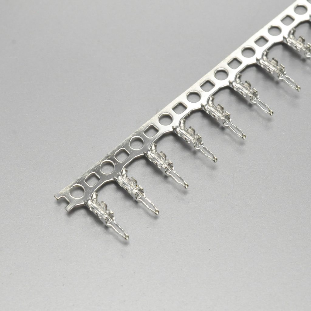
KR1502 180° straight terminal

KR1502 90° right-angle terminal
The housing range: 2 to 16 circuits, and a dimensional detail worth checking
KONNRA’s engineering drawing publishes fifteen housing part numbers, from 2 to 16 circuits:
| Circuits | Part No. | A (mm) | B (mm) | JST A | JST B |
|---|---|---|---|---|---|
| 2 | H150201020101A |
1.50 | 3.70 | 1.5 | 4.0 |
| 3 | H150201030101A |
3.00 | 5.20 | 3.0 | 5.5 |
| 4 | H150201040101A |
4.50 | 6.70 | 4.5 | 7.0 |
| 5 | H150201050101A |
6.00 | 8.20 | 6.0 | 8.5 |
| 6 | H150201060101A |
7.50 | 9.70 | 7.5 | 10.0 |
| 7 | H150201070101A |
9.00 | 11.20 | 9.0 | 11.5 |
| 8 | H150201080101A |
10.50 | 12.70 | 10.5 | 13.0 |
| 9 | H150201090101A |
12.00 | 14.20 | 12.0 | 14.5 |
| 10 | H150201100101A |
13.50 | 15.70 | 13.5 | 16.0 |
| 11 | H150201110101A |
15.00 | 17.20 | 15.0 | 17.5 |
| 12 | H150201120101A |
16.5 | 18.70 | 16.5 | 19.0 |
| 13 | H150201130101A |
18.00 | 20.20 | 18.0 | 20.5 |
| 14 | H150201140101A |
19.50 | 21.70 | — | — |
| 15 | H150201150101A |
21.00 | 23.20 | — | — |
| 16 | H150201160101A |
22.50 | 24.70 | — | — |
The A dimensions match JST exactly at every circuit count. That is the dimension that governs whether the part fits your footprint, and on this parameter the cross-reference is a like-for-like replacement.
The B dimension is 0.30mm smaller across the entire range. On JST’s 2-circuit housing, B is 4.0mm; on the KR1502 it is 3.70mm. The same 0.30mm offset holds all the way up to 13 circuits.
That 0.30mm is exactly the stated general tolerance on KONNRA’s drawing (X.X ±0.30), and JST’s own note on its layout drawing specifies ±0.03mm for all centers, non-cumulative, while giving no separate B tolerance in the published extract. So this is most likely a difference in what each drawing chose to nominate as the nominal, sitting inside tolerance — not a mismatch. But if your enclosure, a neighbouring component, or a wire routing channel is dimensioned against a 4.0mm B on a 2-circuit part, verify it rather than assuming, because you would be 0.30mm tighter than you planned.
Worth stating clearly: JST’s housing list ends at 13 circuits; KONNRA’s runs to 16. Those three extra positions — 14, 15 and 16 — have no direct JST counterpart in the published SZN range. If you need them, they are KONNRA’s own extensions, and they should be qualified as such.
KONNRA also publishes a 7-circuit housing variant with a lengthened partition, part number H150201070102A, drawn separately as 1502H02-A-S. If your application separates adjacent circuits for creepage or for wire routing, that variant exists as a distinct orderable part rather than as a note.
KR1502 housing — 2 to 16 circuits
KR1502 7-circuit housing with lengthened partition
How to identify whether your connector is a JST SZN
The 1.5mm pitch class is crowded, and the SZN is the one that gets misidentified most often, because a housing that has been soldered to a board does not obviously look different from a housing that plugs into a header. Work through these in order — the first one is decisive.
1. Is there a wafer? Look at the board. If there is a separate header soldered down, with a housing that plugs onto it, this is not an SZN. If the housing itself is soldered directly to the board and the crimped terminals push in from above, it is a board-in connector — and in this pitch class, that means the SZN family. This single question resolves most cases.
2. What is the mounting height? The SZN’s published mounting height is 4.25mm, with a thickness of 2.4mm. Measure to the top of the housing from the board surface. A wire-to-board connector in the same pitch class will normally sit higher once mated.
3. Measure the pitch, on centres, across several positions. 1.5mm rules out the 1.25mm and 1.2mm families (DF13, DF14, PicoBlade, Pico-EZmate, ACH) and the 2.0mm and 2.5mm families (PH, XH). At 1.5mm you are still choosing between the SZN, the ZH, the GH, and several Molex systems — go back to question 1.
4. Read any markings on the housing. JST’s numbering for this series is explicitly 2P-SZN through 13P-SZN. If you can read the circuit count followed by -SZN, you are done. KONNRA’s equivalents carry part numbers in the H150201 family.
5. Check what the wire does at the connector. The crimped terminal is inserted into the housing and retained by the housing lances. There is no second connector half to unplug. If your harness disconnects by pulling a plug off a header, you are looking at a wire-to-board series, not this one.
6. If the board is accessible, measure the board thickness. The SZN is specified for 0.6 to 1.2mm PCB thickness. A board outside that window is evidence that either this is not the connector, or that the connector was used outside its specification. Either finding is worth knowing.
SZN vs the rest of the 1.5mm class
The most common error we see is treating every 1.5mm connector as interchangeable with every other 1.5mm connector. Here is how KONNRA’s published cross-reference entries sort out — figures as they appear on KONNRA’s own 1.5mm pitch index, so this is the supplier’s own published positioning:
| KONNRA series | Cross-references to | Architecture | Current | Voltage | Circuits |
|---|---|---|---|---|---|
| KR1502 | JST SZN 1.5 | Board-in | 1A | 200V (page) / 50V (spec) | 2–16p |
| KR1501 | JST ZH 1.5 | Wire-to-board | 1A | 100V | 2–16p |
| KR1506 | JST GH 1.5 | Wire-to-board | 1A | 50V | 2–6p |
| KR1500 | Molex Pico SPOX 1.5 | Wire-to-board | 2.5A | 250V | 2–15p |
| KR1507 | Molex Clik Mate 1.5 | Wire-to-board | 3A | 100V | 2–15p |
| KR1507 (dual row) | Molex Clik Mate 1.5 | Wire-to-board | 1.5A | 100V | 2*4–2*20p |
Two observations that fall straight out of this table.
The KR1502 is the only board-in part in the entire 1.5mm class. Everything else in the list is wire-to-board. So if you have confirmed a board-in architecture, you have already narrowed the field to this one series — which is useful, because it means the identification question is answerable from the board alone.
The 200V entry is anomalous within KONNRA’s own catalogue. The other two JST-replacement entries on the same page publish 100V (ZH) and 50V (GH). A 1.5mm connector sitting at 200V would be an outlier in its own product family — and its own specification sheet says 50V. That is one more reason to treat the page’s 200V as the number to question, not the number to design to.
Also worth noting for anyone comparing current figures across the table: the SZN’s 0.7A (JST) sits below every other entry on that list. The 1.5mm pitch class reaches 2.5A and 3A elsewhere, and it reaches those figures on wire-to-board systems with a different contact architecture. Do not carry a current figure from one row of this table to another.
Crimping and tooling
A board-in connector lives or dies on the crimp, because the crimp is the only electrical joint on the wire side. JST publishes the tooling chain explicitly:
| Terminal | Crimping machine | Crimp applicator | Dies | Applicator with dies |
|---|---|---|---|---|
SZN-002T-P0.7K |
AP-K2N |
MKS-L |
MK/SZN-002-07 |
APLMK SZN002-07 |
SZN-003T-P0.7K |
AP-K2N |
MKS-L |
MK/SZN-003-07 |
APLMK SZN003-07 |
JST notes: “Contact JST for fully automatic crimping applicator.”
KONNRA publishes the crimp dimensions for the same wire range in its specification, which gives you a target to measure against whichever applicator you run:
| Crimp parameter | 26 AWG | 28 AWG | 30 AWG |
|---|---|---|---|
| Crimp width (conductor) | 0.9 ± 0.1 | 0.9 ± 0.1 | 0.9 ± 0.1 |
| Crimp height (conductor) | 0.65–0.75 | 0.58–0.67 | 0.53–0.62 |
| Crimp width (insulation) | 1.10 max | 1.10 max | 1.10 max |
| Crimp height (insulation) | 1.25 max | 1.20 max | 1.05 max |
| Crimp strength | 2.27 kgf min | 1.36 kgf min | 0.9 kgf min |
| Stripping length | 1.1–1.5mm | 1.1–1.5mm | 1.1–1.5mm |
Two things stand out.
The conductor crimp height window is narrow — 0.10mm wide at 26 AWG, and it moves down as the wire gets thinner. This is why the insulation O.D. window matters so much: if the insulation is oversized, the crimp tool cannot close to the specified height, and the crimp strength figure becomes theoretical.
Crimp strength falls steeply with wire size — from 2.27 kgf at 26 AWG to 0.9 kgf at 30 AWG. If you are running mixed gauges in one housing, the pull-test acceptance criterion differs per circuit. A single “pull test the harness” instruction will not be correct for all positions.
Mechanical and environmental performance
The values below are from the KONNRA KR1502 product specification, with the test standards cited as published. This is a more complete qualification set than the original series publishes, which is useful — a cross-reference part is only worth specifying if it has been tested to something, and this one names its standards.
Initial electrical performance
| Item | Test condition | Requirement |
|---|---|---|
| Contact resistance (§5.1) | Dry circuit, 20mV max, 100mA max, measured A–B region (EIA-364-23C) | 20mΩ max |
| Insulation resistance (§5.2) | 500V DC for 1 minute between adjacent contacts (EIA-364-21B) | 500MΩ min |
| Dielectric strength (§5.3) | 500V AC for 1 minute between adjacent terminals or terminal-to-ground (EIA-364-20A) | No breakdown, no flashover |
| Temperature rise (§7.1) | Carrying rated current load (EIA-364-70B) | 30°C max |
Mechanical performance
| Item | Test condition | Requirement |
|---|---|---|
| Terminal insertion force (§6.1) | Insert the crimped terminal into the housing | 0.5 kgf (4.9N) max |
| Terminal/housing retention (§6.2) | Axial pull-out at 25.4 ± 3mm/min | 1.0 kgf (9.8N) min |
The retention figure is worth sizing against your environment. 9.8N minimum is the force required to pull a correctly crimped and seated terminal out of the housing. In a vibration environment, that is the margin you are relying on to keep the wire attached — and unlike a wire-to-board connector, there is no latch or lock holding the wire in place. This is the design consequence of the board-in architecture, and it is the reason the vibration test below is run rather than assumed.
Environmental performance
| Item | Test condition | Requirement |
|---|---|---|
| Vibration (§7.32) | 1.5mm P-P, 10→55→10 Hz in 1 minute, 2 hours in each of X, Y, Z (EIA-364-28B) | No damage · contact resistance 40mΩ max · discontinuity 1 microsecond max |
| Shock (§7.3) | 490 m/s² (50g), 3 strokes in each of 6 directions (EIA-364-27B) | No damage · contact resistance 40mΩ max · discontinuity 1 microsecond max |
| Heat resistance (§7.4) | 105 ± 2°C, 96 hours (EIA-364-17B) | No damage · contact resistance 40mΩ max |
| Cold resistance (§7.5) | −40 ± 2°C, 96 hours (EIA-364-59) | No damage · contact resistance 40mΩ max |
| Thermal shock (§7.7) | −40°C 30 min → RT 5 min → +105°C 30 min → RT 5 min, 5 cycles (EIA-364-32B) | No damage · contact resistance 40mΩ max |
| Humidity (§7.6) | 40 ± 2°C, 90–95% RH, 96 hours (EIA-364-31B) | No damage · contact resistance 40mΩ max · must meet §5.3 · insulation resistance 100MΩ min |
| Salt spray (§7.8) | 35 ± 2°C, 5 ± 1% NaCl, 24 hours (EIA-364-26B) | No damage · contact resistance 40mΩ max |
| Solderability (§7.9) | 245 ± 5°C, 3 ± 0.5 seconds (EIA-364-52) | ≥95% of immersed area free of voids and pin holes |
| Solder resistance (§7.10) | Terminal tip in solder bath at 250°C max, 3–5 seconds, 0.8mm from tip (EIA-364-71B) | No damage |
The discontinuity figure is the one to take seriously. The vibration and shock tests both require interruption of no more than 1 microsecond. That is a genuine electrical-continuity requirement during mechanical excitation, not just a “no visible damage” check. For a connector whose retention depends on a friction fit between a terminal and a housing lance, passing that is the qualification that matters most.
The humidity test relaxes the insulation resistance from 500MΩ to 100MΩ minimum after 96 hours at 90–95% RH. That is a specified allowance, not a failure, and it is normal — but it is a reminder that the 500MΩ headline applies to a dry part.
The solder acceptance window is 245°C for 3 seconds for solderability, and the part survives a 250°C solder bath for 3–5 seconds. Both sit comfortably inside a standard lead-free reflow profile for the board side, but if your process runs hotter or longer at the connector, the margin is thinner than the headline numbers suggest.
Where a board-in 1.5mm connector is the right answer — and where it is not
Board-in connectors solve a specific problem. Because the choice eliminates a whole assembly interface, it is worth being explicit about what that problem is, so you can tell quickly whether it is yours.
The right fit
The harness is terminated once and stays terminated. In an appliance, an instrument, or a power supply where the wire bundle is routed at build time and never disconnected in service, the board-in architecture removes an entire connector half, its footprint, its placement step and its mating interface. All four of those are cost and failure modes you do not take on.
Board area or assembly steps are the constraint. A board-in housing occupies roughly its own body footprint. There is no surrounding keep-out for a mating latch and no second placement. When the board is dense, or when the assembly line is the bottleneck, this is a directly measurable saving.
The wire exit angle needs to be controlled. This is where the KR1502’s two terminal orientations earn their place. A 90° terminal exits the wire parallel to the board, which can keep a bundle inside a low-profile enclosure and reduce the mechanical leverage a wire applies to the terminal body. A 180° terminal exits perpendicular, which suits a cable leaving the board through a housing opening directly above it.
The circuit is low-voltage and low-current. This family’s whole envelope — 0.7A on the original, 1A on the KR1502, and a 1.5mm pitch — is built for signal and small power distribution, not for anything that needs to move meaningful current.
The environment is vibration-exposed but the harness is secured. The series is qualified for 2 hours per axis at 1.5mm peak-to-peak and for 50g shock, with continuity held to within 1 microsecond. That qualification only converts into field reliability if the harness is supported — see the routing section below.
The wrong fit
The harness has to be disconnected in service. This is the clearest disqualifier. On a board-in connector the wire side has no latch, and the disconnection point is the terminal-to-housing interface. Repeatedly pulling crimped terminals in and out of a housing is not a mating cycle, and neither datasheet publishes a durability rating for it. If a technician needs to unplug something, this is the wrong architecture — use a wire-to-board series such as the KR1501 (JST ZH 1.5) or the KR1500 (Molex Pico SPOX 1.5).
You need a positive lock. There is no latch here. Retention is the terminal’s friction fit in the housing, specified at a 1.0 kgf (9.8N) minimum pull-out. That is a real figure and it is tested — but it is a friction fit, and it is not a lock. If your requirement is written as “positive locking connector,” this series does not satisfy it.
You are close to the current limit. At 0.7A on the original and 1A on the KR1502, there is not much room. And because the rating is bounded by a 30°C maximum temperature rise, a design that runs near the limit needs its own rise measurement on its own board — trace geometry changes the answer.
The application is genuinely cold. If the original JST SZN’s −25°C low limit is already a problem in your requirements, that is a reason to look at the KR1502 rather than a reason to avoid it — its −40°C cold test is a real extension. But if your requirement is below −40°C, this family is not the answer at either end.
The board is outside 0.6–1.2mm. That is JST’s specified applicable PCB thickness for the SZN. A 1.6mm board is outside it.
Designing the PCB footprint for a board-in connector
On a wire-to-board design, the header datasheet gives you a footprint and you are done. On a board-in design, the connector is the footprint, so a few extra parameters land on your layout engineer’s desk.
Board thickness is a connector parameter. JST specifies 0.6 to 1.2mm. The solder tails have a fixed length designed for that range. A board outside it is a design review item, not a rounding error.
JST’s own layout drawing comes with three notes, and the third is the one to read twice:
- “The above figure is the figure viewed from soldering side.” Board-in footprints are frequently drawn from the solder side. Confirm the mirroring before you release tooling — this is the single most common layout error on this architecture.
- “Tolerances are non-cumulative: ± 0.03 mm for all centers.” Non-cumulative is the important word. The error does not accumulate across 16 positions, so the tolerance applies per pitch rather than to the total length.
- “Hole dimensions differ according to the type of PC board and piercing method. The dimensions above should serve as a guideline. Contact JST for details.”
That third note is JST telling you directly that the published hole dimensions are a guideline, not a specification, and that hole geometry depends on your board material and your drilling or punching process. If you are releasing a footprint for production, that is a conversation worth having with your connector supplier rather than a dimension worth copying from a PDF.
KONNRA’s drawing supplies a general tolerance block — X.X ± 0.30 · X.XX ± 0.20 · X.XXX ± 0.10 · angle ± 2° — which is applied across the housing dimension table. Note how that compares with JST’s ±0.03mm per center: the two documents are expressing tolerance in different ways (a per-center figure versus a general block), so they are not a like-for-like comparison. But a 0.30mm general tolerance on a 1.5mm-pitch connector is worth knowing about if your assembly depends on tight lateral alignment — and it is exactly the tolerance band that the 0.30mm B-dimension difference sits inside.
Process temperature. The part is qualified for 245 ± 5°C for 3 ± 0.5 seconds of solderability and survives a 250°C solder bath for 3–5 seconds measured 0.8mm from the terminal tip. Confirm where your reflow profile puts the connector during the soak and peak zones; a small board-in housing is much closer to the process temperature than a large header with thermal mass.
Where the connector sits in the process order. Because the housing is soldered to the board, everything downstream of that reflow step now has the housing on it — including any conformal coating, washing, or depaneling operation. If a process step is hostile to a PA66/UL94V-0 housing, that step has to be planned around the connector, not the other way round.
KR1502 board-in housing — the housing itself is the board-side part
Wire routing and strain relief: the part nobody writes down
Here is the design consequence of the board-in architecture that gets skipped most often, because it does not appear on any datasheet as a warning.
There is no latch on the wire side. A wire-to-board connector typically holds the mated pair together with a friction lock or a positive latch, and the housing holds the terminals. On a board-in connector, the housing-to-board joint is a solder joint and the terminal-to-housing joint is a friction fit specified at 1.0 kgf (9.8N) minimum pull-out. There is nothing else.
So the entire retention story is: the terminal is crimped to the wire to a specified crimp strength, the terminal is inserted into the housing and held by the housing lances, and the housing is soldered to the board. Every mechanical load the harness sees in the field arrives at that chain.
What that means in practice:
Anchor the bundle. Put a tie-down, a clip, or a mounting point on the bundle within a short distance of the connector, so that vibration, thermal cycling and handling loads are taken by the harness support rather than by the terminals. The 9.8N retention figure is generous for a terminal this size — but it is a pull-out figure measured on a single terminal in a controlled test, not a rating for a 16-circuit bundle being swung around inside an enclosure.
Route for the exit angle you chose. The 90° terminal exits parallel to the board and the 180° terminal perpendicular to it. Matching the routing to the terminal orientation keeps the wire’s natural bend away from the terminal body. Forcing a 90° terminal into a cable run that wants to leave vertically puts a permanent side load on the crimp.
Keep the bundle’s weight off the connector. On a multi-circuit housing, the bundle gets stiff and heavy quickly. A service loop tied back to the chassis is what keeps that mass from becoming a load path into the housing lances.
Remember what the vibration test actually proves. Two hours per axis at 1.5mm peak-to-peak, with continuity held to within 1 microsecond — that is a statement about a correctly assembled, correctly supported connector. It is not a statement about an unsupported harness. The test is the evidence that the design can hold continuity; the strain relief is what makes it hold in your product.
Plan the assembly sequence. Terminals are inserted into the housing from above, and the housing is fixed to the board. Getting the insertion order and the wire dress right before the bundle is tied off is far easier than correcting it afterwards — particularly on the 16-position housing where the bundle has the least freedom to move.
From reel to finished board: assembly and inspection notes
The published test data in this series is unusually complete, and most of it converts directly into acceptance criteria you can measure on the line. That is worth using — a cross-reference part is far easier to qualify when the supplier has told you the numbers to check.
Incoming inspection
Count and identify against the part numbers, not the description. The terminal’s rating is encoded in its ordering code — SZN-**002**T-P**0.7**K tells you the wire range and the current class before you open the bag. On the KR1502 side, the housing part numbers run H1502010X0101A where X encodes the circuit count, and the terminal order codes carry a Type 01 / Type 02 suffix that distinguishes standard from long bodies. Those two suffixes are easy to transcribe wrongly on a purchase order and impossible to spot by eye once the parts are loose.
Check the materials against the part number. The 180° KR1502 terminal is phosphor bronze and the 90° terminal is brass. If a receipt mixes them, a visual check will not separate them reliably — the finish is the same tin plate on both. Segregate by part number, not by appearance.
Confirm the reel quantity. JST ships the 002 terminal at 14,000 per reel and the 003 at 15,000. KONNRA ships the 180° KR1502 terminal at 15,000 and the 90° at 10,000. A wrong reel count is a silent under-delivery.
Crimp setup and verification
Set the applicator to the published crimp dimensions and verify by measurement rather than by looking at the crimp:
| Wire | Conductor crimp height | Conductor crimp width | Pull strength (min) |
|---|---|---|---|
| 26 AWG | 0.65–0.75mm | 0.9 ± 0.1mm | 2.27 kgf |
| 28 AWG | 0.58–0.67mm | 0.9 ± 0.1mm | 1.36 kgf |
| 30 AWG | 0.53–0.62mm | 0.9 ± 0.1mm | 0.9 kgf |
Measure the crimp height with a crimp micrometer across the conductor barrel, and set the insulation crimp separately — its limits are 1.10mm width and 1.25 / 1.20 / 1.05mm height for 26 / 28 / 30 AWG. Strip length is 1.1 to 1.5mm.
Pull-test per gauge, not per harness. The minimum pull strength falls from 2.27 kgf to 0.9 kgf across the wire range — a factor of two and a half. On a mixed-gauge housing, a single acceptance figure will either pass bad crimps at 26 AWG or reject good ones at 30 AWG.
Watch the insulation window. This is where the JST and KONNRA specifications diverge, and it is the failure that looks like a tooling problem. If your wire insulation measures above 1.0mm, the tool cannot close to the specified conductor crimp height, and the pull strength you measure will sit below the table without anything obviously wrong. Measure the wire, not the wire’s catalogue page.
Terminal insertion and seating
Insertion force is specified at 0.5 kgf (4.9N) maximum for a correctly crimped terminal going into the housing. Two practical consequences:
- A terminal that needs more than that is not seating correctly — check crimp height before you force it.
- A terminal that drops in with no resistance should be checked too. The housing lances are what produce the retention, and retention is specified at 1.0 kgf (9.8N) minimum on axial pull-out at 25.4 ± 3mm/min. Every assembly should have that engagement feel.
Verify retention by sampling, not by inspection. The 9.8N figure is measurable, and it is the single mechanical property that stands between a correctly assembled connector and a wire that works loose in the field. JST’s phrasing on the same feature — “the housing lances facilitate insertion of contacts” — describes the same mechanism.
Solder joints and the board interface
The housing is soldered to the board, so the connector’s reliability is now partly a soldering-process question:
- Solderability is specified as 245 ± 5°C for 3 ± 0.5 seconds, with at least 95% of the immersed area free of voids and pin holes.
- Solder resistance is specified as 250°C maximum for 3 to 5 seconds, measured 0.8mm from the terminal tip.
- The applicable board thickness is 0.6 to 1.2mm.
Beyond that, the joint is a normal through-hole solder joint and should be inspected as one — but with one extra consideration. Because the housing is the connector, a solder defect at a housing tail is not a header you can replace. It is a board rework. That raises the value of inspecting this joint properly at first article, and of confirming your hole geometry before production — which is exactly why JST’s own layout drawing says the published hole dimensions are “a guideline” and directs you to contact them.
First-article checklist
| # | Check | Acceptance |
|---|---|---|
| 1 | Housing part number and circuit count | Matches the drawing (2–16 positions available) |
| 2 | Terminal part number, orientation and Type suffix | 180° / 90°, Standard / Long, as specified |
| 3 | Wire gauge and measured insulation O.D. | AWG #26–#30; insulation within the applicable window |
| 4 | Strip length | 1.1–1.5mm |
| 5 | Conductor crimp height and width | Per the gauge table above |
| 6 | Insulation crimp height | 1.25 / 1.20 / 1.05mm max by gauge |
| 7 | Crimp pull strength | 2.27 / 1.36 / 0.9 kgf min by gauge |
| 8 | Terminal insertion force | ≤ 0.5 kgf (4.9N) |
| 9 | Terminal retention | ≥ 1.0 kgf (9.8N) |
| 10 | Housing seated flat on the board | No gap, no tilt, tails fully through |
| 11 | Solder joints | Full fillet, no voids; process within 245 ± 5°C / 3 ± 0.5s for solderability |
| 12 | Board thickness | 0.6–1.2mm as specified by JST |
| 13 | Continuity and contact resistance | ≤ 20mΩ initial per contact pair |
| 14 | Insulation resistance and dielectric withstand | ≥ 500MΩ min; 500V AC for 1 minute with no breakdown or flashover |
Items 8, 9 and 11 are the ones that catch the assembly problems that pass visual inspection. Item 13 is the one that catches a crimp that closed on insulation instead of conductor — a defect that will pass a continuity buzzer and fail in the field.
Cross-reference checklist: ten things to verify before you substitute
Work through these in order. Each one corresponds to a specific difference or unverified point identified in this guide.
| # | Check | Why |
|---|---|---|
| 1 | Confirm the current your circuit actually draws, then compare against 0.7A — not 1A | The original series is rated 0.7A. The replacement publishes 1A. Design to the lower figure unless you have your own test data. |
| 2 | Get the working voltage confirmed in writing | The KR1502 page publishes 200V while its own specification sheet says 50V. Ask for the controlled figure before you document either. |
| 3 | Measure your wire’s insulation O.D. | JST’s 002 terminal accepts 0.8–1.1mm; the KR1502 publishes 1.0mm max. A 1.05mm wire is inside one window and outside the other. |
| 4 | Confirm your circuit count exists in both ranges | JST publishes 2–13. The KR1502 publishes 2–16. Positions 14–16 have no JST counterpart. |
| 5 | Check your PCB thickness against 0.6–1.2mm | Board thickness is a connector parameter on a board-in part. The KR1502 does not publish a figure, so ask. |
| 6 | Verify the B dimension against your layout | The KR1502’s B is consistently 0.30mm smaller than JST’s across the whole range. Inside tolerance, but only if your layout assumed it. |
| 7 | Confirm you want the substitution at all if the application is a cold one | JST’s low-temperature limit is −25°C; the KR1502 is tested to −40°C. This is a case where the alternative may genuinely be better — verify against your real requirement. |
| 8 | Decide the terminal orientation before you order | KR1502 offers 180° (phosphor bronze) and 90° (brass) terminals. Different alloys, different reels, different layouts. |
| 9 | Confirm the terminal variant matches your wire gauge | The 90° and 180° terminals are drawn as AWG #28–#30, narrower than the series-level AWG #26–#30. AWG #26 needs confirmation against the specific part number. |
| 10 | Ask which document is controlled | PS-KR1502-01 carries a document number, an edition (A1) and a date. Use it as the reference, and ask for written confirmation wherever the drawing or the web page disagrees with it. |
A supplier who will answer items 2, 5 and 10 quickly and in writing is a supplier you can qualify. Those three are the ones where the answer is not already public in a way you can rely on.
Frequently asked questions from procurement and engineering
Is the KR1502 a drop-in replacement for the JST SZN? Mechanically it is close: same 1.5mm pitch, same board-in architecture with no wafer, and the A dimensions match JST exactly across the 2-to-13 circuit range. Electrically it is not identical — the substitutions differ on current rating, on published voltage rating, on temperature range and on the insulation O.D. window. Treat it as a documented cross-reference to be qualified, not as a pin-compatible drop-in.
Can I use it at 1A? The KR1502’s own specification states 1A at 26 AWG, and it publishes a 30°C maximum temperature rise test behind that rating. If you are designing a new product to the KR1502, 1A at 26 AWG is the number to design to. If you are replacing a JST SZN, remember that the part it replaces was rated 0.7A — so a 0.9A circuit was already outside the original specification, and the substitution does not fix that.
What is the actual voltage rating? JST publishes 50V AC/DC for the SZN. KONNRA’s specification sheet §4.0 says 50V. KONNRA’s engineering drawing and product page say 200V. We recommend requesting written confirmation of the controlled figure. Operationally, this family is a low-voltage, low-current connector, and the 50V reading is the one that agrees with both the original series and the controlled specification document.
Do I need a wafer or header? No. That is the defining feature of the series — and KONNRA’s own part-number table lists Wafer: None. You order housings and terminals only. This also means you skip a header placement step and its footprint.
Which terminals do I need? For JST: SZN-002T-P0.7K for AWG #28–#26 (insulation 0.8–1.1mm) or SZN-003T-P0.7K for AWG #30–#28 (insulation 0.7–0.9mm). For the KR1502: the 180° terminal T1502VPT010*A (phosphor bronze) or the 90° terminal T1502RBT010*A (brass), both published at AWG #28–#30 with insulation up to 1.0mm.
How many mating cycles does it have? Neither datasheet publishes a mating-cycle rating for this series. That is consistent with the architecture: the terminal-to-housing interface is not designed as a repeated mate-and-unmate cycle, and on a board-in connector the wire side is not intended to be plugged and unplugged as a routine operation. If your application requires frequent disconnection at this interface, that requirement needs to be raised with the supplier rather than inferred from a number.
What are the lead time and MOQ? KONNRA can deliver complete connector set samples within 45 days. Connector production lead time is typically 2–3 weeks, and wiring harness assemblies are quoted separately. MOQ depends on the housing position count and terminal type — send the specific configuration and it will be quoted against the actual part numbers.
Which standards does it carry? JST’s SZN is UL Recognized (E60389) and CSA Certified (LR20812), and is RoHS2 compliant. KONNRA’s KR1502 specification does not publish a UL or CSA file number. If your product requires a recognised component, ask for the certification status of the specific KR1502 part numbers you intend to use.
What is the difference between the KR1502 and the KR1501? Different originals and different architectures. The KR1502 cross-references the JST SZN 1.5 and is the board-in part. The KR1501 cross-references the JST ZH 1.5 and is a wire-to-board part with a wafer. They share a 1.5mm pitch and nothing else. See our JST ZH 1.5 connector guide for the other series.
Start your cross-reference check
Send us the four things below and we will come back with a specific answer rather than a catalogue page:
- Your actual measured current per circuit, and the number of circuits loaded at once
- Your wire: AWG, conductor construction, and measured insulation O.D.
- Your board: thickness, and the footprint dimensions you are working to (particularly the B dimension)
- The JST part numbers you are replacing, or a photo of the housing from above
From that we can confirm the housing position count, the terminal variant and orientation, the crimp specification, and — where a figure in our published material is ambiguous — give you a written answer against the controlled specification.
- Request a quote — KR1502 pricing, MOQ and configuration for your position count and wire gauge
- Request a sample — complete connector set samples delivered within 45 days
- Request a cross-reference verification — KR1502 against your specific JST SZN part numbers, including insulation O.D., board thickness and position count
- Request the documents — engineering drawing (PDF), product specification PS-KR1502-01 (PDF), package specification (PDF)
- Request a crimp specification sheet — conductor and insulation crimp heights, widths and pull-strength requirements for 26, 28 and 30 AWG
- Request a vendor qualification pack — test capability summary, quality documentation and certification status
- Request assembled harnesses — KR1502 board-in assemblies crimped and tested to the specification above
- Submit a drawing for review — we will flag any specification mismatch before you commit tooling
Contact KONNRA Electronics
- Phone: (86)-769-85449875
- Email: info@konnra.com
- Address: No.6 Nanchang South Road, Chijiao, Wangniudun, Dongguan, Guangdong, China
- Contact us
Orderable components: KR1502 Housing · KR1502 Housing 7P · KR1502 180° Terminal · KR1502 90° Terminal
➡️ Explore the full 1.5mm pitch range · Board-In connector category · How board-in connectors reduce PCB waste · JST connector cross-reference: 20+ series
Sources and method
This guide compares the original manufacturer’s published documentation with KONNRA’s own published documentation for the cross-reference part. Where the two disagree, both figures are shown and the discrepancy is stated rather than resolved by preference.
Original manufacturer (JST) — SZN series:
- JST SZN connector datasheet (
eSZN.pdf), JST product documentation — board-in architecture and 4.25mm mounting height / 2.4mm thickness; current rating 0.7A AC/DC (AWG #26); voltage rating 50V AC/DC; temperature range −25°C to +85°C including temperature rise; insulation resistance 500MΩ min; applicable wire AWG #30 to #26; withstanding voltage 500V AC/minute; applicable PCB thickness 0.6–1.2mm; UL Recognized E60389 and CSA Certified LR20812; RoHS2. Contact table forSZN-002T-P0.7KandSZN-003T-P0.7Kincluding wire ranges, insulation O.D. windows and reel quantities; terminal material and finish; crimp tooling chain (AP-K2N, MKS-L, MK/SZN-002-07, MK/SZN-003-07, APLMK SZN002-07, APLMK SZN003-07). Housing table2P-SZNto13P-SZNwith A and B dimensions, 1,000 pieces per bag, PA 66 UL94V-0 natural (white). Model-number allocation rules (002/003, T, P, K). PC board layout notes: ±0.03mm tolerance for all centers, non-cumulative. - Current rating 0.7A AC/DC (AWG #26) and voltage rating 50V AC/DC independently confirmed against two further renderings of the same JST specification set.
Cross-reference manufacturer (KONNRA) — KR1502 series:
- Product specification PS-KR1502-01, Rev/Edition A1, issued and revised 2022/2/26, Engineering Dept., Dongguan Konnra Electronics Co., Ltd. Used for: part-number table (housing
H150201**0101A, terminalsT1502VPT010*A/T1502RBT010*A, wafer: none); materials and surface treatment; §4.0 ratings (rated voltage 50V AC/DC, rated current 1A at 26 AWG, ambient −40°C to +105°C, applicable wire AWG 26–30 with insulation O.D. 1.0mm max); §5.1 contact resistance 20mΩ max; §5.2 insulation resistance 500MΩ min; §5.3 dielectric strength 500V AC / 1 minute; §6.1 terminal insertion force; §6.2 terminal/housing retention; §6.3 crimp specification for 26/28/30 AWG; §7.1 temperature rise; §7.3 shock; §7.4 heat resistance; §7.5 cold resistance; §7.6 humidity; §7.7 thermal shock; §7.8 salt spray; §7.9 solderability; §7.10 solder resistance; §8.0 remark. - Engineering drawing, KR1502 series, Rev A3, drawing numbers 1502H01-A-S (housing), 1502H02-A-S (housing 7P), 1502TV01-A-S (180° terminal), 1502TR01-A-S (90° terminal), 1502TR02-A-S (90° terminal, lengthened). Used for: the 2–16 circuit housing dimension table (fifteen part numbers); the 200V AC, DC voltage rating published in the drawing’s SPECIFICATIONS block; housing 7P part number
H150201070102A; terminal ordering codes, materials (phosphor bronze / brass), wire ranges (AWG #28–#30), insulation O.D. (1.0mm max) and reel quantities (15,000 / 10,000); general tolerance block X.X ±0.30 / X.XX ±0.20 / X.XXX ±0.10. - KR1502 product page (both published variants) and the 1.5mm pitch index page. Used for: the page specification table (pitch 1.50mm, circuits 2–16pin, current 1A, voltage 200V); the Overview prose figure (“rated at 1A and 50V”); component page links; document download links; and the published cross-reference positioning of the sibling 1.5mm series (KR1501, KR1506, KR1500, KR1507) used in the comparison table.
Not published in any source reviewed: mating-cycle (durability) rating for the JST SZN or the KONNRA KR1502; contact resistance for the SZN in JST’s own rating set; applicable PCB thickness for the KR1502; UL/CSA file numbers for the KR1502. These are stated as not published rather than estimated. The KR1502 page and its specification sheet also disagree on the voltage rating, and neither document states which is controlled — that question is flagged for written confirmation rather than resolved here.
Method note. Figures were taken from controlled documents where available and from published web pages only where no controlled document exists. Dimensional comparisons were made by transcribing both tables and differencing the values position by position; the 0.30mm B-dimension offset was found to hold consistently across all twelve overlapping circuit counts, and is reported as observed rather than characterised as a design change. Temperature, current and voltage figures were compared only where both sources publish the same parameter on the same basis; where a parameter is published at a qualified condition in one source and unqualified in the other, the qualification is stated in the comparison.