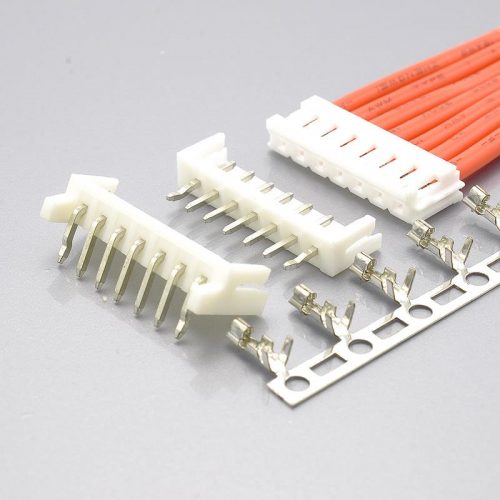
Quick answer: The HIROSE DF3 is a 2mm-pitch, single-row, wire-to-board connector for discrete wire — 3A per pin at 22–24 AWG, 250V AC/DC, −55°C to +105°C, 2 to 15 positions, certified to UL E52653 and CSA LR95109. The KONNRA KR2009 is its cross-reference equivalent in the DIP (through-hole) form: same 2.00mm pitch, same 2–15 positions, same 250V rating, same 650V withstanding voltage, same 30mΩ initial contact resistance — and, as this article shows, the same housing length and width at every one of the fourteen position counts.
Two numbers on the original datasheet will decide whether this part actually suits your design, and neither is the headline figure.
The first: HIROSE’s own UL/CSA rated voltage for the DF3 is 30V AC/DC, not 250V. The 250V figure is the general rating. If your design needs an agency-recognised voltage, the DF3’s is 30V — and the KONNRA side does not publish one at all.
The second: HIROSE rates the DF3 to −55°C. The KONNRA KR2009 is rated to −40°C. Both stop at +105°C. That 15°C difference at the cold end is the single most decision-relevant gap in this cross-reference, and it is easy to miss because the hot end matches exactly.
Everything below is taken from HIROSE’s official DF3 catalogue and KONNRA’s product specification and drawings, both cited at the end.
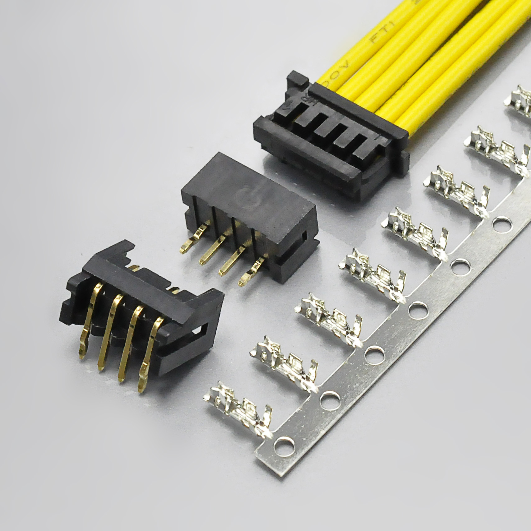
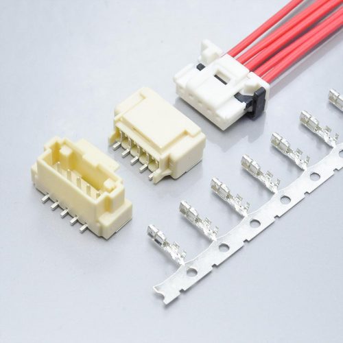
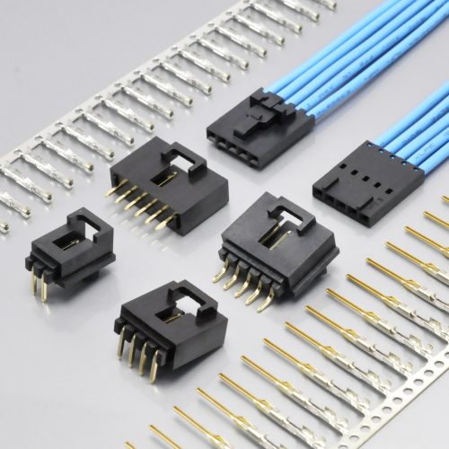
KONNRA KR2009 series 2.00mm pitch DF3 DIP wire-to-board connector, the cross-reference equivalent for the HIROSE DF3
At a glance
| Item | HIROSE DF3 | KONNRA KR2009 |
|---|---|---|
| Pitch | 2mm | 2.00mm |
| Rows | 1 | 1 |
| Positions | 2 – 15 | 2 – 15 |
| Application | Wire-to-board, discrete wire | Wire-to-board |
| Current, crimp | 3A/pin at 22–24 AWG; 2A/pin at 26 AWG; 1A/pin at 28 AWG | 3A (specified at 22 AWG) |
| Voltage, general rating | 250V AC/DC | 250V AC/DC |
| Voltage, UL/CSA rating | 30V AC/DC | Not published |
| Operating temperature | −55°C to +105°C | −40°C to +105°C |
| Operating humidity | 40 to 80% | Not published |
| Storage temperature | −10°C to +60°C | Not published |
| Contact resistance, initial | 30mΩ max | 30mΩ max |
| Insulation resistance | 1,000MΩ min | 1000MΩ min |
| Withstanding voltage | 650V AC for 1 minute | 650V AC / minute |
| Applicable wire | 22 to 28 AWG | AWG 22# – 28# |
| Crimp socket insulator | PA, black, UL94V-0 | PA66, black, UL94 V-0 |
| Pin header insulator | PA, black, UL94V-0 | PA6T, black, UL94 V-0 |
| Crimp contact material | Phosphorous bronze | Phosphor bronze |
| Pin header contact material | Brass | Brass |
| Plating | Tin or gold, chosen by part number | Tin (terminal) and gold (wafer) |
| Mating durability | 30 cycles (tin), 50 cycles (gold) | 30 cycles |
| Agency | UL E52653 / CSA LR95109 | UL E482542 |
| Solder heat, DIP | Flow +260°C for 10 sec | Wave peak 250°C max, 3–5 sec |
| RoHS | Yes | Yes |
Four rows in that table need a note before you read anything else into them.
The current rating is per pin and it depends on the wire. HIROSE publishes three different figures for one connector — 3A at 22–24 AWG, 2A at 26 AWG, 1A at 28 AWG. So “3A” is only true if you are crimping the heavier gauges. The KONNRA specification states its rating as 3A (22 AWG), which is precise, but the KONNRA product page shows a flat “3A” with no gauge attached.
The UL/CSA voltage is a separate, much lower number and it gets its own section below.
The KONNRA operating humidity and storage figures are simply not published — HIROSE gives 40 to 80% operating and −10°C to +60°C storage. If your specification carries storage limits, that is a question to ask rather than assume.
The durability row is not a like-for-like comparison. HIROSE publishes two figures depending on plating; KONNRA publishes one. That also gets its own section.
The number that changes the design: the DF3’s UL/CSA voltage is 30V, not 250V
This is the most consequential thing in HIROSE’s DF3 catalogue, and it is easy to read past because the catalogue prints both numbers in the same specification block without much ceremony.
| HIROSE DF3 rating | Value |
|---|---|
| Rated Voltage (general) | 250V AC/DC |
| UL-CSA Rated Voltage | 30V AC/DC |
| UL, CSA File No. | UL: E52653 / CSA: LR95109 |
The general rating is 250V. The agency rating is 30V. That is a factor of more than eight, and the lower figure is the one that applies when a design has to show a recognised-agency voltage.
It is not a typo and it is not confined to one part. The catalogue prints the UL-CSA block as its own table with its own rated-current column (24 AWG → 3A/pin, 26 AWG → 2A/pin, 28 AWG → 1A/pin), immediately below the general ratings table. Two tables, two sets of numbers, and the agency set is smaller in both dimensions.
What this means in practice, depending on which side of the cross-reference you are standing on:
- If you have a DF3 design and it relies on the 250V figure for a safety file, check whether the agency-recognised voltage — 30V — is what your file actually calls out. A design reviewed on the 250V number may not hold up on the agency number.
- If you are evaluating the KONNRA KR2009, note that KONNRA publishes UL E482542 (on the four component pages) but no UL- or CSA-rated voltage anywhere — not on the product page, not in the specification document, and not on the engineering drawings. The drawings carry a six-line specification block and the voltage line reads “Voltage rating: 250V AC,DC” with no agency qualifier.
So the honest position is this: the KR2009 is UL-listed, and the UL-rated voltage is not published. Given that the original part’s agency voltage is 30V rather than 250V, that is not a detail to leave unresolved. It is a one-question ask to the supplier, and it is the first item on the checklist at the end of this article.
The second number to check: the cold end is 15°C short
Both connectors stop at +105°C. Only one of them starts at −55°C.
| HIROSE DF3 | KONNRA KR2009 | |
|---|---|---|
| Operating temperature range | −55°C to +105°C | −40°C to +105°C |
| Cold-end difference | — | 15°C narrower |
The hot end matching exactly is what makes this easy to miss. A designer comparing the two datasheets sees “+105°C” on both and moves on. The range is anchored at one end and short by 15°C at the other.
Whether that matters depends entirely on where the equipment goes. For the applications HIROSE names for the DF3 — general office automation such as copiers and printers — an indoor, climate-controlled environment makes −40°C and −55°C equally irrelevant, and the gap costs nothing. For anything specified against an outdoor, cold-chain, refrigeration, or transport qualification, a −55°C requirement cannot be met by a part rated to −40°C without re-qualification.
And the underlying test programmes are different, not just the banners. HIROSE’s temperature-cycle test runs −55°C → +85°C, five cycles. KONNRA’s thermal-shock test runs −40°C → +105°C, five cycles. So the two documents are not describing the same test with a different label — HIROSE cycles to a colder floor and a lower ceiling; KONNRA cycles to a warmer floor and a higher ceiling. The KONNRA test is actually the more aggressive one at the hot end.
That is worth stating plainly, because it cuts both ways: the KR2009’s published range is narrower on the cold side, while its thermal-shock test is run to a higher temperature than the original’s. A −40°C to +105°C part tested through +105°C thermal shock is not a weaker part than a −55°C to +105°C part tested to +85°C. It is a differently-qualified part. Match the qualification envelope to your application rather than assuming either is simply “better”.
Where the two systems match — including the dimensions, exactly
The physical overlap here is unusually complete, and one part of it is worth verifying yourself because it is the strongest drop-in evidence in this whole comparison.
| Parameter | HIROSE DF3 | KONNRA KR2009 | Match |
|---|---|---|---|
| Pitch | 2mm | 2.00mm | Exact |
| Number of rows | 1 | 1 | Exact |
| Positions offered | 2 – 15 | 2 – 15 | Exact |
| Application | Wire-to-board | Wire-to-board | Exact |
| Rated voltage (general) | 250V AC/DC | 250V AC/DC | Exact |
| Withstanding voltage | 650V AC / 1 min | 650V AC / minute | Exact |
| Contact resistance, initial | 30mΩ max | 30mΩ max | Exact |
| Insulation resistance | 1,000MΩ min | 1000MΩ min | Exact |
| Flammability | UL94V-0 | UL94 V-0 | Exact |
| Crimp contact material | Phosphorous bronze | Phosphor bronze | Exact |
| Pin header contact material | Brass | Brass | Exact |
| Vibration amplitude | 0.75mm half-amplitude | 1.5mm peak-to-peak | Exact (same figure) |
| Vibration duration | 2 hours in each of 3 directions | 2 hours in each of X, Y and Z | Exact |
| Discontinuity limit | 1μs | 1 microsecond max | Exact |
One line in that table is worth reading a second time, because the two documents state it in different units. HIROSE specifies vibration as a half amplitude of 0.75mm; KONNRA specifies 1.5mm P-P. Half amplitude is half of peak-to-peak, so 0.75mm half-amplitude is 1.5mm peak-to-peak. The two are the same number expressed two ways, not two different requirements. Verify it in that form rather than treating “0.75” and “1.5” as a mismatch.
The dimensions match to the last digit
This is the part worth checking on your own screen.
HIROSE’s catalogue tabulates the crimp socket dimensions for every position count. KONNRA’s housing drawing tabulates the same two dimensions for the same positions. Both are in millimetres. Here they are side by side:
| Positions | Hirose DF3-#S-2C: A | KONNRA H20090: A | Hirose: B | KONNRA: B |
|---|---|---|---|---|
| 2 | 6 | 6.00 | 2 | 2.00 |
| 3 | 8 | 8.00 | 4 | 4.00 |
| 4 | 10 | 10.00 | 6 | 6.00 |
| 5 | 12 | 12.00 | 8 | 8.00 |
| 6 | 14 | 14.00 | 10 | 10.00 |
| 7 | 16 | 16.00 | 12 | 12.00 |
| 8 | 18 | 18.00 | 14 | 14.00 |
| 9 | 20 | 20.00 | 16 | 16.00 |
| 10 | 22 | 22.00 | 18 | 18.00 |
| 11 | 24 | 24.00 | 20 | 20.00 |
| 12 | 26 | 26.00 | 22 | 22.00 |
| 13 | 28 | 28.00 | 24 | 24.00 |
| 14 | 30 | 30.00 | 26 | 26.00 |
| 15 | 32 | 32.00 | 28 | 28.00 |
Every value agrees. All twenty-eight numbers.
And the agreement is not coincidental — both tables follow the same two linear laws:
- A = 2.00 + 2.00 × positions — 6.00mm at two positions, 32.00mm at fifteen
- B = 2.00 × (positions − 1) — 2.00mm at two positions, 28.00mm at fifteen
B is simply the pin-row span, which is what a 2.00mm pitch forces: fifteen positions span fourteen pitches. But A — the overall housing length — matching at every size is a real design statement. The end walls are the same thickness in both parts at every position count, which is what makes a replacement sit in an existing opening without touching the layout.
The same drawing publishes the tolerances these dimensions are held to, which is more than many series drawings bother to do:
| Decimal places | Tolerance |
|---|---|
| X.X | ±0.30 |
| X.XX | ±0.20 |
| X.XXX | ±0.10 |
| Angle | ±2° |
| Units | mm |
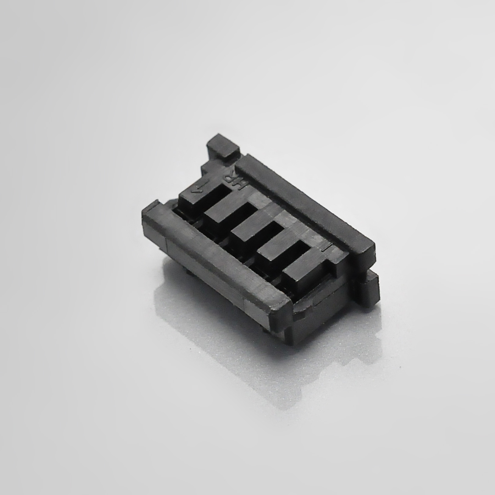
KONNRA KR2009 2.00mm housing, the cross-reference for the HIROSE DF3 crimp socket
One dimension that cannot be compared, and it is a relevant one. HIROSE describes the crimp socket as a “low profile design with mounting height 7.5mm“, and the DF3 catalogue gives 6.6mm and 7.5mm as the two heights in the range. The KONNRA housing and wafer drawings I was able to read give length and width ladders but no mounting height figure in extractable text. So the height comparison — the one that decides whether a replacement clears the enclosure above the board — is not established here. Measure it, or ask for it.
The cross-reference on this part is unambiguous — and that is worth saying
It is worth pausing on something that is a genuine improvement over how this supplier documents other series.
All four KONNRA component pages for this series state the compatible series outright:
| KONNRA component | KONNRA page | Stated as compatible with |
|---|---|---|
| Housing | components/2009-h | DF3 Series |
| Terminal | components/2009-t | DF3 Series |
| Right Angle Wafer | components/2009-dip90 | DF3 Series |
| Straight Wafer | components/2009-dip180 | DF3 Series |
There is no “N/A” here, no unnamed equivalent, and no need to reverse-engineer the cross-reference from a component code. The product page title says it, the category listing says it, and every component page says it. If you have been burned by a cross-reference table that names the target vaguely, this series is the opposite case.
The mapping onto HIROSE’s own part structure is exact, too. HIROSE encodes the header form in the part number:
| HIROSE suffix | Meaning | KONNRA equivalent component |
|---|---|---|
| DSA | Straight dip pin header | Straight Wafer (2009-dip180) |
| DS | Right angle dip pin header | Right Angle Wafer (2009-dip90) |
| (socket) | Crimp socket | Housing (2009-h) |
| (contact) | Socket contact | Terminal (2009-t) |
So a DF3-#P-2DSA maps to the KONNRA straight wafer, and a DF3-#P-2DS maps to the right angle wafer. Those are the two forms KONNRA makes.
And here is the scope limit you need to know before you plan around it. HIROSE’s DF3 range is wider than the DIP headers. The catalogue’s mating-combination diagram lists seven connector types:
| HIROSE DF3 type | Part number form | KONNRA KR2009 offers it? |
|---|---|---|
| Straight pin header (DIP) | DF3(A)-#P-2DSA |
Yes |
| Right angle pin header (DIP) | DF3(A)-#P-2DS |
Yes |
| Straight pin header (SMT) | DF3#-#P-2V |
No |
| Right angle pin header (SMT) | DF3#-#P-2H |
No |
| In-line plug | DF3-#EP-2C |
No |
| In-line plug with panel lock | DF3AA-#EP-2C |
No |
| Crimp socket | DF3#-#S-2C |
Yes |
KONNRA covers three of those seven rows: the crimp socket and the two DIP headers. The SMT headers and the in-line plugs — including the panel-lock wire-to-wire version — are outside the KR2009 range.
That is not a fault in the KR2009; it is a DIP part, as its name and its product page both say. But “KR2009 replaces DF3” is too broad a statement to act on. If your DF3 design uses an SMT header (-2V or -2H) or an in-line plug (-EP), the KR2009 is not the replacement, and no amount of pitch matching changes that. Check the suffix first.
The right angle wafer has three different part numbers across two documents
This is the one item in this comparison that can put a wrong part on a purchase order, so it is worth setting out in full.
KONNRA publishes a product specification and a series drawing for this part. Both describe the right angle DIP wafer. Here is the right angle wafer’s part number as each document prints it:
| Document | Where | Part number as printed |
|---|---|---|
Product specification PS-KR2009-01, section 2.0 |
Wafer row | C2009RD***10G0101PA |
Series drawing, DF3 DIP 90° Wafer sheet |
Ordering Code block | C2009RD***10G0101RA |
Series drawing, DF3 DIP 90° Wafer sheet |
Title block, PART NO.: |
C2009RD***10T0101RA |
Three strings, two of which differ from each other by a single character, and the third differs in two places.
Read the differences carefully, because they are not the same difference:
- The specification says
10G0101PA - The drawing’s ordering code says
10G0101RA - The drawing’s title block says
10T0101RA
So the seventh character from the end is G in two places and T in one, and the final two characters are PA in the specification and RA in both places on the drawing.
The two documents do not agree, and one of the two documents does not even agree with itself. The drawing’s title block and its own ordering code are different strings on the same sheet.
The straight wafer, by contrast, is consistent
Worth noting, because it shows the problem is localised rather than a general sloppiness:
| Document | Where | Straight wafer part number |
|---|---|---|
| Product specification, section 2.0 | Wafer row | C2009VD***10G0101RA |
Series drawing, DF3 DIP 180° Wafer sheet |
Ordering Code block | C2009VD***10G0101RA |
Series drawing, DF3 DIP 180° Wafer sheet |
Title block, PART NO.: |
C2009VD***10G0101RA |
The straight wafer’s part number is identical in all three places. So this is one part number that has been mis-transcribed, not a systemic problem with the document set.
How the inconsistency most likely arose — and why it still matters
Both wafer drawings carry a revision block with exactly one entry:
| Revision entry | Description |
|---|---|
| 2020.05.25 | “Change the part number and frame format” |
The only recorded revision to these drawings is a part-number change. That is consistent with what you would expect to see if a part number was revised in 2020 and every reference to the old and new forms was not updated at the same time — the ordering code updated in one place and not the title block, or vice versa, and the specification carried a form that predates the change.
I am labelling that as the likely explanation, not a documented fact. The documents do not say which of the three strings is current.
What to do about it: do not order the right angle wafer from a printed part number. Quote the drawing number instead — the right angle wafer sheet is drawing 2009WRD101-A-S, and the straight wafer is 2009WVD101-A-S, both at REV A2 — and ask KONNRA to confirm the current part number in writing. The straight wafer’s part number can be used as printed; the right angle one cannot.
The full set of part numbers, for reference:
| Component | Part number | Drawing number | Revision |
|---|---|---|---|
| Housing | H20090***0201A |
2009H101-A-S |
A2 |
| Terminal | T20090PT0101A |
2009T101-A-S |
A2 |
| Straight wafer (DIP 180°) | C2009VD***10G0101RA |
2009WVD101-A-S |
A2 |
| Right angle wafer (DIP 90°) | disputed — see above | 2009WRD101-A-S |
A2 |
The housing and terminal part numbers agree between the specification and the drawings, so only the right angle wafer is affected.
Reading the circuit code
All four part numbers encode the position count the same way, and the convention is worth knowing because it is not the number you might expect:
| Field | Values |
|---|---|
| Position code | undefined = 2 positions, undefined = 15 positions |
| Insulator material (housing) | undefined = PA66 black V0 (the only code published) |
So the code is a literal 1 followed by the zero-padded position count — 102 for two, 115 for fifteen, and ten positions would be 110. This is the same convention this supplier uses across its connector families, so it is worth learning once.
And note the housing ordering code publishes exactly one insulator material: 01: PA66 Black V0. There is no second material code and no colour option — the KR2009 housing is available in black only, which matters if your assembly relies on colour to prevent cross-mating.
One character is missing from a flammability grade
A smaller item, but it lands in the field a compliance reviewer reads first.
The two wafer sheets both state the insulator material. On the straight wafer sheet it reads:
Insulator: PA6T UL 94V-0
On the right angle wafer sheet it reads:
Insulator: PA6T UL 94V-
The flammability grade on the right angle wafer sheet is truncated — undefined instead of undefined. The trailing zero is missing.
Two things make this worth a sentence rather than a shrug. First, the truncated string appears on the sheet whose part number is already the one in dispute, so a reviewer working from that sheet is getting two defects at once. Second, the material line itself is otherwise correct and agrees with the straight wafer and with the specification, so this is a transcription slip rather than a genuine material difference — the part is PA6T UL94 V-0, as the specification section 3.0 and the component pages both confirm.
Where the two systems differ
Beyond the two headline numbers, there are several differences that matter to a design review.
| Parameter | HIROSE DF3 | KONNRA KR2009 | Nature of the difference |
|---|---|---|---|
| Operating temperature, cold end | −55°C | −40°C | 15°C narrower |
| Operating temperature, hot end | +105°C | +105°C | Same |
| UL/CSA rated voltage | 30V | Not published | Unresolved on the KONNRA side |
| Current rating vs wire gauge | 3A / 2A / 1A by gauge | 3A at 22 AWG | KONNRA states the 22 AWG case only |
| Mating durability | 30 cycles tin / 50 cycles gold | 30 cycles | KONNRA publishes the lower figure |
| Contact resistance after environmental test | 30mΩ max, unchanged | 40 or 60mΩ max | KONNRA 1.3× to 2× looser |
| Insulation resistance after humidity | 500MΩ min | 100MΩ min | KONNRA 5× looser |
| Temperature cycle envelope | −55°C to +85°C | −40°C to +105°C | Different envelope |
| Solder heat, DIP | +260°C for 10 sec | peak 250°C max, 3–5 sec | KONNRA 10°C cooler, shorter |
| Crimp socket insulator | PA (grade unspecified) | PA66 | KONNRA more specific |
| Pin header insulator | PA (grade unspecified) | PA6T | KONNRA more specific |
| Plating choice | Tin or gold, by part number | Tin (terminal) + gold (wafer) | Fixed split, not a choice |
| Header forms offered | DIP and SMT, plus in-line plugs | DIP only | Scope gap |
| Positions in catalogue | 2 – 15 | 2 – 15 | Same |
Five of these deserve more than a table cell.
The durability figure is lower on the KONNRA side — and it may be understated
HIROSE publishes the DF3 mating durability as two numbers, selected by plating:
| Plating | HIROSE rated mating durability |
|---|---|
| Tin plating | 30 times |
| Gold plating | 50 times |
KONNRA publishes one number: 30 cycles, in specification section 7.1.
Now look at what the KR2009’s mating interface actually is. KONNRA’s terminal is phosphor bronze, tin plated over nickel, and its wafer contact is brass, gold plated over nickel. The mating pair is therefore tin against gold.
So the question “which durability applies?” has no published answer for the KR2009 — and the interesting part is the direction of the uncertainty. If the gold surface governs, the capability is 50 cycles and KONNRA has published the more conservative 30. Either way, the published 30-cycle figure is the one to design against until the supplier says otherwise, but a gold-bearing interface being rated at the tin figure is a plausible case of the document understating its own part rather than overstating it.
The environmental acceptance limits are looser on the KONNRA side
HIROSE and KONNRA both run the standard environmental suite, and both express the outcome as a contact-resistance limit. The limits are not the same:
| Test | HIROSE DF3 limit | KONNRA KR2009 limit |
|---|---|---|
| Initial | 30mΩ max | 30mΩ max |
| After humidity (96 h, +40°C, 90–95% RH) | 30mΩ max | 40mΩ max |
| After temperature cycling | 30mΩ max | 40mΩ max |
| After mating durability | 30mΩ max | 60mΩ max |
| Insulation resistance after humidity | 500MΩ min | 100MΩ min |
HIROSE holds its contact-resistance limit flat at 30mΩ across every environmental test. KONNRA permits the resistance to rise. The two insulation-resistance figures after humidity differ by a factor of five.
This is not a defect in either document — a post-conditioning acceptance limit is a legitimate engineering choice, and a looser limit can reflect a harsher test rather than a worse part. But it does two things you should account for:
- You cannot read “30mΩ” off both datasheets and conclude the parts are equivalent. They are equivalent as supplied. After 96 hours at 90–95% relative humidity they are specified differently.
- The KONNRA figure you should design against in a humid application is 100MΩ, not the 1000MΩ on the product page. See the next section.
The solder-heat window is narrower
For a DIP part, the through-hole soldering process window is a real constraint, and the two documents give different windows:
| HIROSE DF3, DIP type | KONNRA KR2009 | |
|---|---|---|
| Wave / flow soldering | +260°C for 10 sec | peak 250°C max, 3–5 sec |
| Hand soldering | soldering iron +300°C for 2 sec | not published |
| Pre-heat | not published | 150–180°C |
| Time above 217°C | not published | 60–150 sec |
HIROSE’s DIP qualification is 260°C for 10 seconds. KONNRA’s published wave-soldering profile peaks at 250°C max for 3–5 seconds. So KONNRA’s stated process window is 10°C cooler and materially shorter.
If your wave-solder process runs a 260°C peak — which the original part is qualified for — then the KR2009’s published profile does not cover it, and you either adjust the profile or qualify the part outside its published window. That is a process-engineering decision, not a drop-in substitution, and it is the kind of thing that surfaces at pilot build rather than at design review.
The KR2009 specification also adds something HIROSE’s catalogue does not publish for the DF3: an explicit solderability requirement — soldering time 3 ± 0.5 seconds at 245 ± 5°C, with 95% of the immersed area required to show no voids or pin holes. That is a useful acceptance criterion to have in writing.
The plating arrangement is different in kind, not just in degree
HIROSE offers plating as a choice, selected in the part number: the contact suffix None means tin plating, A means gold plating on the plug contact, and C means gold plating on the socket contact. So you pick.
KONNRA fixes the split by component: the wire-side terminal is tin over nickel; the board-side wafer contact is gold over nickel. You do not choose — the arrangement is built into which component you order.
That is a legitimate and common architecture (a gold board interface with a tin wire interface), and for many applications it is the sensible one. But it means a DF3 design that specified gold on both sides maps to a KR2009 that is gold on one side only, and that is a change to the contact system, not just to a part number.
One more thing about the plating: the two KONNRA documents describe it differently
KONNRA’s specification section 3.0 says the wafer contact is:
Gold Plated Over Nickel
KONNRA’s product page and all four component pages say:
Gold flash over Nickel
“Gold flash” and “gold plated” are not the same thing. A flash is a very thin cosmetic deposit; a specified plating implies a controlled thickness. These are contact surfaces, so the distinction is functional rather than semantic.
The documents disagree, and none of them gives a thickness figure — HIROSE’s catalogue does not publish one for the DF3 either. So if the gold thickness on the board interface matters to you, it is not answerable from any document on either side. Ask for it.
The force table: two exact laws and a constant
Section 8.0 of the KONNRA specification publishes insertion force and withdrawal force for every position count from 2 to 15, at initial and after 30 mating cycles. It is a clean table, and unusually well behaved.
The insertion force follows one exact law
| Positions | 2 | 3 | 4 | 5 | 6 | 7 | 8 | 9 | 10 | 11 | 12 | 13 | 14 | 15 |
|---|---|---|---|---|---|---|---|---|---|---|---|---|---|---|
| I.F. max (kgf) | 3.00 | 3.50 | 4.00 | 4.50 | 5.00 | 5.50 | 6.00 | 6.50 | 7.00 | 7.50 | 8.00 | 8.50 | 9.00 | 9.50 |
All fourteen published values are reproduced exactly by:
I.F. = 2.00 + 0.50 × positions
At two positions, 2.00 + 1.00 = 3.00. At fifteen, 2.00 + 7.50 = 9.50. There is no exception anywhere in the table.
The reading is straightforward: 2.00 kgf of housing engagement that does not change with size, plus 0.50 kgf per contact. A constant per-contact term means the insertion force you measure on a two-position sample predicts the fifteen-position force exactly, so you do not need to build the worst case to size a fixture.
The withdrawal force follows a second exact law
| Positions | 2 | 3 | 4 | 5 | 6 | 7 | 8 | 9 | 10 | 11 | 12 | 13 | 14 | 15 |
|---|---|---|---|---|---|---|---|---|---|---|---|---|---|---|
| R.F. min, initial (kgf) | 0.50 | 0.70 | 0.90 | 1.10 | 1.30 | 1.50 | 1.70 | 1.90 | 2.10 | 2.30 | 2.50 | 2.70 | 2.90 | 3.10 |
All fourteen values are reproduced exactly by:
R.F. = 0.10 + 0.20 × positions
At two positions, 0.10 + 0.40 = 0.50. At fifteen, 0.10 + 3.00 = 3.10. Again, no exception.
So the withdrawal force is a fixed 0.10 kgf of baseline plus 0.20 kgf per contact — and the per-contact withdrawal force is exactly 40% of the per-contact insertion force (0.20 against 0.50). That ratio being constant across the whole range is what you want to see: it means the contact behaves consistently with size rather than the geometry changing character as positions are added.
After 30 cycles the force drops by a constant 0.10 kgf
| Positions | 2 | 3 | 4 | 5 | 6 | 7 | 8 | 9 | 10 | 11 | 12 | 13 | 14 | 15 |
|---|---|---|---|---|---|---|---|---|---|---|---|---|---|---|
| R.F. min, initial (kgf) | 0.50 | 0.70 | 0.90 | 1.10 | 1.30 | 1.50 | 1.70 | 1.90 | 2.10 | 2.30 | 2.50 | 2.70 | 2.90 | 3.10 |
| R.F. min, after 30 cycles (kgf) | 0.40 | 0.60 | 0.80 | 1.00 | 1.20 | 1.40 | 1.60 | 1.80 | 2.00 | 2.20 | 2.40 | 2.60 | 2.80 | 3.00 |
| Difference | 0.10 | 0.10 | 0.10 | 0.10 | 0.10 | 0.10 | 0.10 | 0.10 | 0.10 | 0.10 | 0.10 | 0.10 | 0.10 | 0.10 |
The loss is 0.10 kgf at every single position count — identical in all fourteen rows, not a percentage and not a growing penalty.
Two things follow. First, the retention loss is a constant force, not a fixed proportion, so it matters most at the small sizes: 0.10 kgf out of 0.50 is a 20% loss at two positions, while 0.10 out of 3.10 is barely 3% at fifteen. If you are designing a two-position interconnect, that is a fifth of your retention gone after 30 matings, and it is the small sizes where the published numbers are tightest. Second, because the loss is constant and the table is otherwise exact, you can interpolate with confidence at any position count — the whole table is reproducible from two formulas.
An honest note on this table versus the same supplier’s other series
This table is worth contrasting with its counterpart in the KONNRA wire-to-wire series, which publishes the same kind of table for insertion and withdrawal force by position count. That one has a row that does not fit its own progression, and it prints the after-30-cycles column as identical to the initial column at every size — which reads as zero retention loss.
This table has neither problem. All forty-two published values are reproduced exactly by the two laws and the constant loss, and the after-30-cycles column is genuinely lower than the initial column rather than copied from it. It is a well-constructed table, and it is reasonable to rely on it.
The terminal numbers put the withdrawal force in perspective
Three figures from specification section 6.0 reframe what the withdrawal numbers mean:
| Item | Section | Value |
|---|---|---|
| Terminal insertion force | 6.2 | 1.0 kgf (9.8 N) max, per terminal |
| Terminal / housing retention force | 6.3 | 1.0 kgf (9.8 N) min, per terminal |
| Pin retention force | 6.4 | 1.0 kgf (9.8 N) min, per pin |
A single terminal is required to resist at least 1.0 kgf of axial pull before it leaves its housing. Compare that against the force needed to unmate the complete connector:
| Positions | Whole-connector withdrawal (kgf) | Aggregate minimum terminal retention (kgf) | Ratio |
|---|---|---|---|
| 2 | 0.50 | 2.0 | 4.0 × |
| 8 | 1.70 | 8.0 | 4.7 × |
| 15 | 3.10 | 15.0 | 4.8 × |
The connector unmates at roughly a quarter to a fifth of the force its terminals can withstand — a ratio of about 4 to 5 across the range, widening slowly with position count.
This is a materially different situation from some other series in the same catalogue, where the equivalent ratio runs to tens rather than single digits. Here the retention capability is much closer to the withdrawal force, which means two practical things: the mating interface is still the intended release point, so a wire will not pull out before the connector separates — but the margin is not enormous, and the pin retention figure matters in a way it does not on a lower-force design. If a harness is pulled sideways off a board, a 1.0 kgf minimum pin retention is the number that decides whether the header pin stays in the wafer or leaves with the wire.
Note also what section 6.4 adds that earlier generations of this document did not carry: an explicit pin retention requirement. That is the board-side counterpart to terminal retention and it is the right thing to specify on a DIP header, where the pins are pressed into the wafer rather than moulded in.
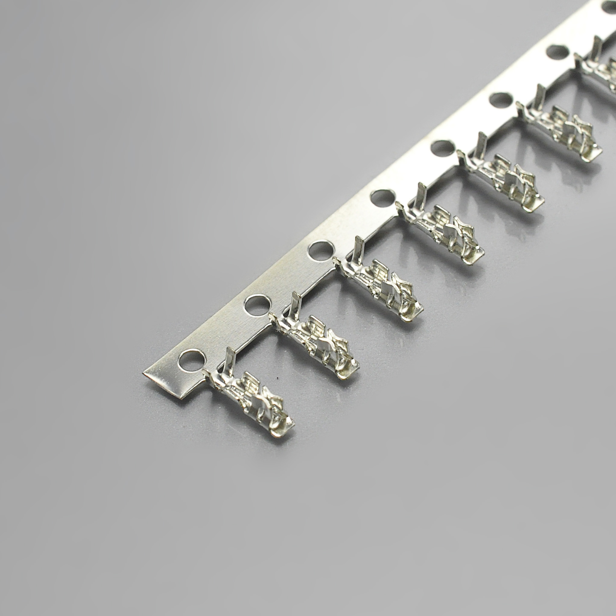
KONNRA KR2009 2.00mm terminal, the cross-reference for the HIROSE DF3 crimp contact
One wording inconsistency in that block is worth flagging, since it affects how you would run the test. Section 6.4’s Chinese text says the pin is pulled out; the English text in the same cell says “Apply axial push force”. One of those is a mistranslation. Given the item measures retention, the pull-out reading is the sensible one, but if you are writing a test procedure from this document, specify the direction yourself rather than copying the English.
Crimp and terminal data
The crimp table covers four wire gauges, one more than the equivalent table in this supplier’s wire-to-wire series. That extra row is the 22 AWG line, which is also the gauge the 3A rating depends on.
| 22 AWG | 24 AWG | 26 AWG | 28 AWG | |
|---|---|---|---|---|
| Conductor crimp width | 1.30 ± 0.10 | 1.30 ± 0.10 | 1.30 ± 0.10 | 1.30 ± 0.10 |
| Conductor crimp height | 0.85 ± 0.05 | 0.80 ± 0.05 | 0.75 ± 0.05 | 0.70 ± 0.05 |
| Insulation crimp width | 1.60 max | 1.60 max | 1.60 max | 1.60 max |
| Insulation crimp height | 1.70 ± 0.05 | 1.55 ± 0.05 | 1.40 ± 0.05 | 1.30 ± 0.05 |
| Crimp strength, min | 4.54 kgf | 3.63 kgf | 2.27 kgf | 1.36 kgf |
| Stripping length | 1.6 – 2.1 mm | 1.6 – 2.1 mm | 1.6 – 2.1 mm | 1.6 – 2.1 mm |
Four things to take from it.
The conductor crimp height is a clean, uniform ladder. 0.85 → 0.80 → 0.75 → 0.70. Every step is exactly 0.05mm, across all four gauges. That is the pattern you want: one tool-height increment per gauge step, the same increment throughout, so a single dial setting change covers each move and the middle gauges are true midpoints. Note this is not universal — the equivalent table in this supplier’s wire-to-wire series steps by 0.10mm and then 0.05mm, so do not assume the ladder carries across series.
The insulation crimp height does not follow the same ladder. 1.70 → 1.55 → 1.40 → 1.30. The steps are 0.15, 0.15, then 0.10 — not uniform, and not the same increment as the conductor ladder. So the conductor crimp height and the insulation crimp height move by different amounts as you change gauge, and neither is derivable from the other. Set each from the table.
Crimp strength falls faster than the copper at the thin end. 4.54 kgf at 22 AWG down to 1.36 kgf at 28 AWG is a factor of 3.3. The conductor cross-section from 22 AWG to 28 AWG falls by a factor of about 4. So the pull-out requirement does not quite track the copper — the requirement falls slightly more slowly than the cross-section, which means the thin gauges carry a marginally higher relative demand than the thick ones. That is a conservative direction to be wrong in, and it is why 28 AWG is the gauge to qualify first if your harness covers the whole range.
The stripping length is a single range for all four gauges: 1.6 to 2.1 mm. That is a 0.5mm window — narrower than the 0.6mm window this supplier publishes on its wire-to-wire series, so a strip setting that works there may fall outside the window here. Verify the setting against this table rather than carrying one over.
And the reel quantity, which appears on the terminal drawing rather than in the specification: 15,000 pieces per reel for the terminal T20090PT0101A.
Materials and plating: which component gets which
This is where the KONNRA documentation is at its weakest, and where a five-minute read of two documents replaces a guess.
The product page lists materials in a single line:
PA66/UL94/PA6T/Brass/Phosphor Bronze
That line contains two different plastics and two different metals, and it does not say which component uses which. The product page’s plating line has the same problem — Gold flash/Tin over Nickel appears without saying which side gets the tin and which gets the gold.
The specification and drawings do resolve it, component by component:
| Component | Base material | Plating | Flammability |
|---|---|---|---|
| Housing (crimp socket) | PA66 | none specified | UL94 V-0 |
| Terminal (crimp contact) | Phosphor bronze | Tin over nickel | not published |
| Wafer insulator (both DIP forms) | PA6T | none specified | UL94 V-0 |
| Wafer contact (both DIP forms) | Brass | Gold over nickel | not published |
Three things follow from putting those documents side by side.
The two plastics are not interchangeable, and the split is deliberate. The wire-side housing is PA66; the board-side wafer is PA6T. PA6T is a higher-temperature polyamide, and the reason it is on the wafer rather than the housing is the process: a DIP wafer goes through wave soldering, so it has to survive solder temperatures while the housing — which is crimped on after the board is processed — never does. That is the correct engineering choice, and the specification makes it explicitly by listing the wafer’s base material separately for both the straight and the right-angle forms.
Both connectors use brass for the header contact and phosphor bronze for the crimp contact, which matches the original exactly. HIROSE’s catalogue lists the pin header contact as brass and the crimp contact as phosphorous bronze. So the contact-material architecture is the same on both sides of this cross-reference, which is a stronger statement than the two parts merely sharing a pitch.
The mixed plating is the deliberate design decision, and it is the one to check against your own requirement. The wire side is tin over nickel; the board side is gold over nickel. As noted earlier, HIROSE offers plating as a choice via part number, so a DF3 design that specified gold on both mating surfaces does not map cleanly onto a KR2009 that is gold on one side only.
The nickel underlayer is worth a sentence, because it is spelled out rather than left as a general “tin plated” or “gold plated” note. On both the tin and the gold side, the nickel is a barrier between the copper alloy and the outer deposit — the layer that keeps the contact from degrading when the outer metal diffuses into the substrate over time and temperature. On a part rated to +105°C that is the correct construction, and it is specified explicitly on both the specification and the drawings.
The environmental programme, and the acceptance limits that disagree
The specification runs eleven environmental and process tests, all referenced to EIA standards. Nine of them are the familiar suite; the last two are the soldering-process pair, which a DIP part needs and which some datasheets omit.
| Test | Condition | Reference | Contact resistance limit |
|---|---|---|---|
| Durability | 30 mating cycles at ≤ 10 cycles/minute | EIA-364-09C | 60 mΩ max |
| Temperature rise | At rated current load | EIA-364-70B | (30°C max instead) |
| Vibration | 1.5mm P-P, 10~55~10 Hz swept in 1 minute, 2 hours in each of X, Y and Z | EIA-364-28B | 60 mΩ max |
| Shock | 490 m/s² (50g), 3 strokes in each of X, Y and Z | EIA-364-27B | 60 mΩ max |
| Heat resistance | 105 ± 2°C for 96 hours | EIA-364-17B | 60 mΩ max |
| Cold resistance | −40 ± 2°C for 96 hours | EIA-364-59 | 60 mΩ max |
| Humidity | 40 ± 2°C at 90–95% RH for 96 hours | EIA-364-31B | 40 mΩ max |
| Thermal shock | −40°C 30 min → room temp 5 min → +105°C 30 min → room temp 5 min, 5 cycles | EIA-364-32B | 40 mΩ max |
| Salt spray | 35 ± 2°C, 5 ± 1% solution, 8 hours | EIA-364-26B | 40 mΩ max |
| Solderability | 3 ± 0.5 seconds at 245 ± 5°C | EIA-364-52 | (95% wetting instead) |
| Solder heat resistance | DIP type, per the wave-soldering profile in section 9.0 | EIA-364-71B | (no damage instead) |
Beyond the table:
| Result | Published limit |
|---|---|
| Temperature rise at rated current | 30°C max |
| Contact resistance, initial | 30mΩ max |
| Contact resistance, after vibration, shock, heat, cold or durability | 60mΩ max |
| Contact resistance, after humidity, thermal shock or salt spray | 40mΩ max |
| Insulation resistance, initial | 1000MΩ min |
| Insulation resistance, after humidity | 100MΩ min |
| Discontinuity under vibration and shock | 1 microsecond max |
| Solderability, wetted area | 95% of immersed area free of voids and pin holes |
Now here is the inconsistency, and it is the kind of thing that quietly changes a test report.
Eight of the eleven tests state a contact-resistance limit. Five of them allow 60mΩ; three of them allow 40mΩ. The grouping is:
- 60mΩ allowed after: durability, vibration, shock, heat resistance, cold resistance
- 40mΩ allowed after: humidity, thermal shock, salt spray
A single-condition heat soak is granted a 50% larger resistance rise than a combined thermal-shock cycle. Both are thermal exposures to the same temperatures — heat resistance is 96 hours at +105°C, and the thermal shock cycle includes 30 minutes at that same +105°C, five times. The thermal shock test is the harsher of the two by any reasonable reading, and it is the one held to the tighter limit.
The same applies to cold: 96 hours at −40°C is allowed 60mΩ, while the thermal shock test that includes −40°C is allowed only 40mΩ.
This is not a contradiction that makes either number wrong — a test programme is allowed to set different acceptance limits for different conditioning, and a defensible reason exists: vibration, shock and pure temperature soak measure mechanical and thermal stability, while humidity, thermal shock and salt spray involve corrosion or condensation, where a lower resistance rise is the more meaningful acceptance. But the document does not say that, and a reader comparing the rows will reasonably ask why the milder soak has the looser limit. If you are writing a qualification plan from this specification, take the limits as written for each test rather than assuming a single “post-conditioning” figure applies — but if you are comparing the part against the HIROSE original, note that HIROSE holds one flat figure of 30mΩ across every environmental test, so neither the 40 nor the 60 matches it.
And note the initial-to-durability step specifically. The initial limit is 30mΩ; after 30 mating cycles it is 60mΩ. The permitted resistance doubles over 30 cycles, which is the same direction the original goes but a larger step: HIROSE allows 30mΩ after its durability test, unchanged from initial. If your application budgets a contact-resistance rise over life, the KR2009 permits twice what it starts with and the DF3 permits none.
Finally, the humidity test derates insulation resistance by a factor of ten. Initial: 1000MΩ min. After 96 hours at 90–95% relative humidity: 100MΩ min. That is a legitimate post-conditioning relaxation, but it is a real one, and the product page does not mention it — the page’s General Specification carries a single insulation-resistance row reading “1000MΩ min” with the post-humidity figure absent. In a humid application the number to design against is the one in section 7.7, not the one on the product page. It is also the row where KONNRA and HIROSE diverge most: after the same 96-hour humidity exposure, HIROSE specifies 500MΩ min against KONNRA’s 100MΩ min.
What is not published
A cross-reference guide is only useful if it says where the documents stop. These are the gaps I could establish, on both sides.
| Not published | Where you would expect it |
|---|---|
| The KONNRA UL- or CSA-rated voltage | The specification has no agency section at all. UL E482542 appears, but only on the four component pages, and no rated voltage is attached to it. Given that the original’s agency voltage is 30V against a 250V general rating, this is the most important single gap in this comparison. |
| Any CSA file number for the KR2009 | HIROSE publishes both UL E52653 and CSA LR95109. No CSA number appears anywhere in KONNRA’s documents. |
| A gold or tin plating thickness | The specification says “Gold Plated Over Nickel” on the wafer; the product page and component pages say “Gold flash over Nickel”; no thickness figure appears on either side. HIROSE’s catalogue does not publish one for the DF3 either. |
| Operating and storage humidity, and storage temperature | HIROSE publishes operating humidity 40–80%, storage temperature −10°C to +60°C and storage humidity 40–70%. KONNRA publishes none of the three. |
| The wafer mounting height | HIROSE states 7.5mm mounting height for the crimp socket and gives 6.6mm and 7.5mm as the range’s two heights. The KONNRA drawings give length and width ladders but no height figure in extractable text. |
| A readable package specification | Package-spec_KR2009.pdf is published and is 318 KB, but its content is graphics rather than text. The only packaging figure available in text is the 15,000 pieces per reel on the terminal drawing. |
| A current derating curve against position count | The 3A rating is per pin at 22 AWG. HIROSE gives the gauge dependence (3A/2A/1A) but neither document gives a curve for the aggregate current a multi-position connector can carry. |
| Terminal and insulator flammability separately | Both documents rate the insulators UL94 V-0. Neither states a flammability rating for the contact materials, which is normal but worth knowing when filling out a material declaration. |
One row in that table deserves emphasis rather than a footnote. The agency voltage gap is not symmetric with the other gaps. Every other missing figure has an equivalent missing on both sides — neither party publishes a plating thickness, so there is nothing to compare. But on the agency voltage, HIROSE publishes a number and it is 30V, while KONNRA publishes none. So you cannot resolve it by reading; you have to ask.
How to identify whether your connector is a DF3
If you are holding an unmarked 2mm wire-to-board connector and no part number, these are the features that separate this family from the many other 2mm connectors on the market.
Confirm the family first:
- 2.00mm pitch, single row, wire-to-board. Wire side is a crimp housing carrying crimped contacts; board side is a header with pins that go through the board. If both halves are cable-mounted, this is a wire-to-wire family, not this one.
- The board half is a through-hole (DIP) header, not a surface-mount one. This is the important discriminator. HIROSE makes the DF3 header in both forms — straight DIP (
-2DSA), right angle DIP (-2DS), straight SMT (-2V) and right angle SMT (-2H). The KONNRA KR2009 covers only the two DIP forms. If the header you are replacing is surface-mount, the KR2009 is not your part, regardless of pitch, position count, and the fact that both are labelled DF3. - Positions run from 2 to 15. That is the full range on both sides.
- Two distinct contact materials in one mated pair. The crimp contact is phosphor bronze, the header pin is brass. If you are told both are the same alloy, the documentation is being simplified.
Then confirm which DIP form you have:
| Form | HIROSE part number form | KONNRA component |
|---|---|---|
| Straight — pins exit perpendicular to the board, mating axis normal to the PCB | DF3(A)-#P-2DSA |
Straight Wafer (2009-dip180) |
| Right angle — pins exit parallel to the board, mating axis along the PCB | DF3(A)-#P-2DS |
Right Angle Wafer (2009-dip90) |
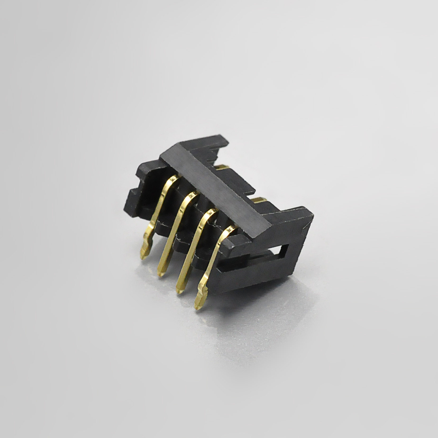
KONNRA KR2009 DIP right angle wafer, the cross-reference for the HIROSE DF3 right angle DIP pin header
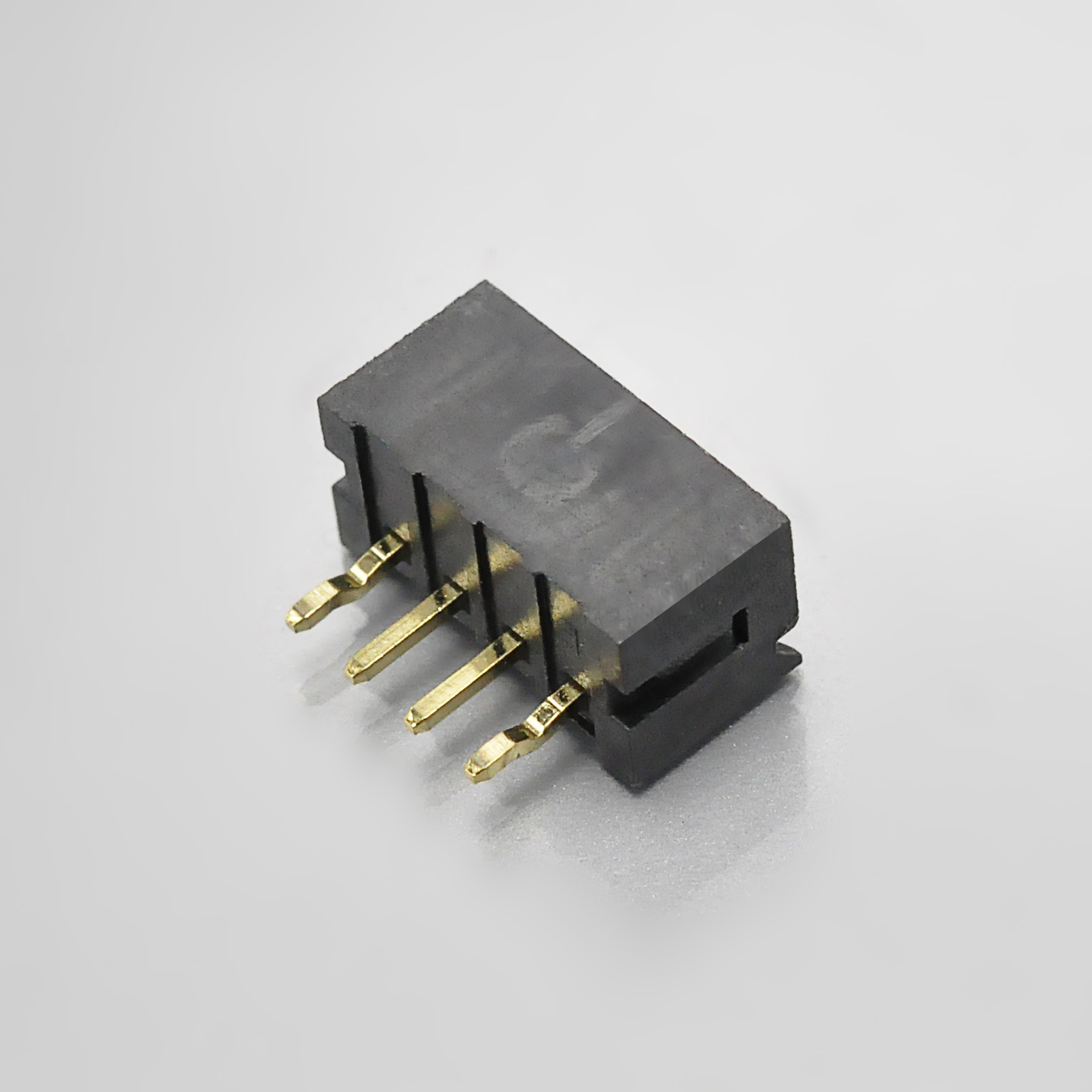
KONNRA KR2009 DIP straight wafer, the cross-reference for the HIROSE DF3 straight DIP pin header
Note the naming convention in the KONNRA component codes, because it is not the same as HIROSE’s: KONNRA names the wafer by its angle designation — 2009-dip90 for the right angle and 2009-dip180 for the straight — while HIROSE names the header by its termination code — DS for right angle and DSA for straight. The component codes agree on the physical geometry, but do not assume the two naming schemes line up character for character.
And confirm the position count from the dimension table rather than by eye. Once you have the overall housing length in millimetres, you can read the position count straight off: positions = (length − 2) ÷ 2, because the housing length follows A = 2.00 + 2.00 × positions. A housing measuring 18.00mm is an eight-position part. That works on both the HIROSE original and the KONNRA equivalent, which is a useful cross-check to have when a label has worn off.
Where the KR2009 sits in the 2.00mm class
This series sits in two taxonomies at once, and both are worth knowing.
Within KONNRA’s HIROSE alternatives category, the page lists four series:
| KONNRA series | HIROSE family | Pitch |
|---|---|---|
| KR2009 | DF3 | 2.0mm |
| KR1256 | DF13 | 1.25mm |
| KR1255 | DF14 | 1.25mm |
| KR1002 | DF19 | 1.0mm |
The category’s pitch filter offers 1.0mm, 1.25mm and 2.0mm, and KR2009 is the only one of the four that is 2.0mm. So if you are looking for a HIROSE cross-reference at 2mm pitch, there is exactly one series to look at, and this is it. That is a clean situation and worth noting, because in the Molex-alternatives category the same supplier has four 2.0mm series that are easy to confuse.
Within KONNRA’s 2.00mm pitch category, the Series filter enumerates nineteen codes. KR2009 is the DF3 entry among them, alongside the four series positioned against Molex 2.0mm families.
The useful thing to carry away is that the HIROSE-alternatives grouping is cleaner than the Molex-alternatives one, and the pitch resolves it. In the Molex set, three series carry the same “mx2.0” string in their title while pointing at three different Molex families. In the HIROSE set, there is no such collision — each series names its family (DF3, DF13, DF14, DF19) and the pitch separates them. Search on the family name, not the pitch alone.
Cross-reference checklist: ten things to verify before you commit
Work through these in order. The first two are where the money is; the rest are the details that surface later if you skip them.
- Establish the UL/CSA-rated voltage on the KONNRA side. HIROSE’s own agency voltage for the DF3 is 30V against a 250V general rating. KONNRA publishes UL E482542 but no agency voltage at all. If your design needs a recognised-agency voltage, this is unresolved until the supplier answers, and it is the first question to ask.
- Check the cold end against your requirement. HIROSE rates the DF3 to −55°C; the KR2009 is rated to −40°C. Both stop at +105°C, which is why the 15°C gap is easy to miss. A −55°C requirement cannot be met from this replacement without re-qualification.
- Confirm which header form you are replacing. The KR2009 covers the DIP headers (
DSAandDS) and the crimp socket. It does not cover the SMT headers (-2V,-2H) or the in-line plugs (-EP), including the panel-lock version. Check the suffix before anything else. - Verify the operating current against your actual wire gauge. HIROSE rates 3A/pin at 22–24 AWG, 2A/pin at 26 AWG and 1A/pin at 28 AWG. KONNRA states 3A at 22 AWG. If you are crimping 26 or 28 AWG, the relevant figure is 2A or 1A, not 3A.
- Decide which durability figure applies and get it confirmed. HIROSE publishes 30 cycles for tin and 50 cycles for gold. KONNRA publishes 30 cycles only, while its wafer contact is gold plated — so the published figure may be the conservative one. Design against 30 until the supplier says otherwise.
- Re-check your contact-resistance budget in the environment you actually run in. Initial resistance matches at 30mΩ. After environmental conditioning, KONNRA permits 40mΩ after humidity, thermal shock or salt spray and 60mΩ after heat, cold, vibration, shock or durability — against HIROSE’s flat 30mΩ. If your budget assumed the original’s flat figure, it does not transfer.
- In a humid application, design against 100MΩ, not 1000MΩ. The specification permits 100MΩ min after 96 hours at 90–95% RH, a ten-fold relaxation that the product page omits — and HIROSE specifies 500MΩ min after the same exposure.
- Compare the wave-solder profile before running a build. HIROSE qualifies the DIP part for +260°C for 10 seconds. KONNRA’s published profile peaks at 250°C max for 3–5 seconds. A 260°C process is outside the KR2009’s published window.
- Do not order the right angle wafer from a printed part number. Three different strings appear across two documents — the specification says
C2009RD***10G0101PA, the drawing’s ordering code saysC2009RD***10G0101RA, and the drawing’s own title block saysC2009RD***10T0101RA. Quote the drawing number2009WRD101-A-Sat REV A2 and ask for the current part number in writing. The straight wafer’s number is consistent and can be used as printed. - Confirm the gold thickness on the board interface, and set the crimp from the tables. The documents say both “gold plated” and “gold flash” with no thickness. Separately, the conductor crimp height ladder steps by 0.05mm per gauge and the insulation ladder by 0.15/0.15/0.10 — they are different ladders, so set each from its own row and note that the stripping window here is 1.6–2.1mm, narrower than this supplier’s wire-to-wire series.
Frequently asked questions
What is the KONNRA KR2009 a replacement for?
The HIROSE DF3 series, in its DIP (through-hole) form. KONNRA’s four component pages for the series all state “Compatible: DF3 Series”, and the mapping is exact: the housing replaces the DF3 crimp socket, the terminal replaces the socket contact, and the two wafers replace the straight and right angle DIP pin headers.
Does the KR2009 cover the whole DF3 range?
No. HIROSE’s DF3 mating-combination diagram lists seven connector types. The KR2009 covers three of them — the crimp socket and the two DIP pin headers. The SMT headers (-2V and -2H) and the in-line plugs (-EP, including the panel-lock version) are not in the KR2009 range. Check the suffix on your DF3 part number before assuming a replacement exists.
Is the KR2009 a drop-in replacement?
Physically, the evidence is strong: the housing length and width match the original at all fourteen position counts, following the same two laws (A = 2.00 + 2.00 × positions, B = 2.00 × (positions − 1)), and pitch, row count, position range, materials and initial electrical ratings all agree. Electrically and environmentally it is not a drop-in — the cold-end temperature rating, the UL/CSA voltage, the post-environmental contact-resistance limits and the wave-solder window all differ. Treat it as a mechanically compatible part needing electrical, thermal and process re-qualification.
What is the DF3’s UL/CSA rated voltage?
30V AC/DC. HIROSE publishes this as a separate “UL-CSA” specification block, distinct from the general rated voltage of 250V AC/DC. The UL file is E52653 and the CSA file is LR95109. The two ratings are more than a factor of eight apart and the agency figure is the one that applies to a recognised-agency design.
What is the KONNRA KR2009’s UL-rated voltage?
It is not published. KONNRA publishes UL file E482542 on its four component pages, but no UL- or CSA-rated voltage appears on the product page, in the specification document, or on the engineering drawings. It is a direct question to the supplier.
Can I use a KR2009 at 3A on any wire gauge?
No. The 3A figure applies at 22 AWG, which is the gauge the KONNRA specification names. HIROSE’s own catalogue makes the dependence explicit: 3A/pin at 22–24 AWG, 2A/pin at 26 AWG, 1A/pin at 28 AWG. The applicable wire range is AWG 22# to 28# with a maximum insulation outside diameter of 1.45mm, so the 26 and 28 AWG cases are within the part’s range but carry lower ratings.
How many mating cycles does it take?
30 cycles, per specification section 7.1, tested at no more than 10 cycles per minute. Note that HIROSE rates the same family at 30 cycles for tin plating and 50 for gold, and KONNRA’s wafer contact is gold plated — so 30 may be conservative, but it is the published figure and the one to design against until confirmed.
Why does the contact resistance limit change between tests?
The specification permits 60mΩ after durability, vibration, shock, heat or cold, but only 40mΩ after humidity, thermal shock or salt spray. The document does not explain the split. Take each test’s limit as published rather than applying a single post-conditioning figure, and note that neither matches HIROSE’s flat 30mΩ limit.
Is the operating temperature the same as the original?
The hot end is identical at +105°C. The cold end is not: HIROSE rates the DF3 to −55°C, KONNRA rates the KR2009 to −40°C. Separate from the ratings, the test programmes also differ — HIROSE cycles −55°C to +85°C and KONNRA −40°C to +105°C, so KONNRA’s thermal-shock test is the more aggressive one at the top end.
Which component is PA66 and which is PA6T?
The crimp housing is PA66; both wafer insulators are PA6T. Both are UL94 V-0 and both black. The split follows the process: the wafer goes through wave soldering and needs the higher-temperature polyamide, while the housing is crimped on after board processing. The product page’s single material line lists both plastics together without saying which is which.
Is the board-side contact really phosphor bronze like the original?
No — and this is a genuine difference in how the materials are documented rather than a difference between the parts. Both connectors use brass for the header contact and phosphor bronze for the crimp contact, so the materials match. But the KONNRA product page lists “Brass” and “Phosphor Bronze” in one line without assigning them, so it is worth reading the specification to see that the wafer contact is brass.
Does it come in any colour other than black?
No. The housing ordering code publishes a single insulator material, 01: PA66 Black V0, and the component pages list the colour as black for every component. If your assembly process relies on colour to prevent cross-mating, this series does not support that method.
Why do two documents disagree about the right angle wafer’s part number?
Both wafer drawings carry exactly one revision entry, dated 2020.05.25, described as “Change the part number and frame format”. That is consistent with a part number having been revised and every reference to it not being updated at once — but the documents do not say which form is current, so I am offering that as the likely explanation rather than a fact. Quote the drawing number (2009WRD101-A-S, REV A2) and ask for written confirmation.
Where can I get the documents?
All the KONNRA documents are linked at the end of this article, including the product specification, the series drawing and the four per-component product drawings. HIROSE’s DF3 catalogue is the primary source for every DF3 figure quoted here.
Start your cross-reference check
If you are holding a DF3 part number on a BOM, the useful next step is not a catalogue search — it is a comparison against your actual requirement, and two facts decide most of it.
- Send the full DF3 part number, including the termination suffix.
-2DSAand-2DSare inside the KR2009 range;-2V,-2Hand-EPare not. That one suffix decides whether this is a conversation or a dead end. - Send your operating temperature range and your wire gauge. The cold-end rating and the per-gauge current rating are the two numbers where the KR2009 and the DF3 do not match, and both are answerable from your own specification in minutes.
Then ask the two questions the documents cannot answer: the KR2009’s UL-rated voltage, and which durability figure applies to a tin-against-gold mating pair.
The four cross-referenced components are the Housing (H20090***0201A, replacing the DF3 crimp socket), the Terminal (T20090PT0101A, replacing the socket contact), the Straight Wafer (C2009VD***10G0101RA, replacing the DSA straight DIP pin header) and the Right Angle Wafer (replacing the DS right angle DIP pin header — confirm the part number in writing). All are 2.00mm pitch, single row, 2 to 15 positions, 3A at 22 AWG, 250V AC/DC, −40°C to +105°C, UL listed to E482542, and RoHS compliant.
Contact KONNRA with the DF3 part number, your wire gauge, your temperature range and your working drawing, and the cross-reference can be confirmed against the part number and the drawing number rather than against the family name.
- View the KONNRA KR2009 2.00mm DF3 DIP wire-to-board connector series
- Download the KR2009 product specification (PS-KR2009-01)
- Download the KR2009 series drawing
- Send an enquiry to KONNRA
Sources and method
Everything in this article comes from manufacturer documents, cited so it can be checked. Where a figure could not be obtained, it is listed as not published rather than estimated.
HIROSE primary document:
- DF3 Series catalogue, “2mm Pitch Connector for Discrete Wire Connection (Product approved by UL CSA Standard)”, dated Apr. 2025, 21 pages —
hirose.com/en/product/document?series=DF3&documenttype=Catalog&lang=en&documentid=en_DF3_CAT. Source of: the rated current by gauge (3A at 22–24 AWG, 2A at 26 AWG, 1A at 28 AWG), the general rated voltage 250V AC/DC, the UL-CSA rated voltage of 30V AC/DC, the UL-CSA rated-current table, UL E52653 and CSA LR95109, operating temperature −55 to +105°C, operating humidity 40–80%, storage −10 to +60°C and 40–70%, insulation resistance 1,000MΩ min at 500V DC, withstanding voltage 650V AC for 1 minute, contact resistance 30mΩ max at 20mV max and 1mA, the vibration specification (10–55 Hz, 0.75mm half amplitude, 2 hours in each of 3 directions, no discontinuity ≥1μs), the humidity test (30mΩ max, 500MΩ min, 96 hours at +40±2°C and 90–95%), the temperature cycle (−55°C to +85°C, 5 cycles), mating durability (tin 30 times, gold 50 times), solder heat resistance (DIP flow +260°C for 10 sec, hand soldering +300°C for 2 sec), the materials and finish table, the product-number structure including theDSA/DS/V/Htermination codes, the mating-combination diagram, and the crimp socket dimension table including the A and B ladders for 2 to 15 positions and the 100-pieces-per-bag purchase unit
KONNRA primary documents:
- Product specification PS-KR2009-01, Rev A1, issued 2022/2/26, 7 pages —
konnra.com/wp-content/uploads/2023/09/PS-KR2009-01.pdf. Source of: the part numbers, the material and plating assignment by component, the ratings, sections 5.0 to 7.0 with all eleven environmental and process tests and their EIA references, the contact-resistance limits of 30/40/60mΩ, the post-humidity insulation resistance of 100MΩ min, the crimp table, the wave-soldering profile, and the section 8.0 insertion and withdrawal force table for 2 to 15 positions - Series drawing KR2009-Series-Drawing.pdf, 4 pages, REV A2, dated 2020 —
konnra.com/wp-content/uploads/2023/09/KR2009-Series-Drawing.pdf. Four sheets:DF3 Housing(2009H101-A-S),DF3 Terminal(2009T101-A-S),DF3 DIP 180° Wafer(2009WVD101-A-S) andDF3 DIP 90° Wafer(2009WRD101-A-S). Source of the housing A and B dimension ladders, the tolerance table, the circuit code, the Housing ordering code, the three conflicting right angle wafer part numbers, the truncated94V-flammability grade on the right angle sheet, the terminal reel quantity of 15,000 PCS, and the RoHS declarations - Package specification
Package-spec_KR2009.pdf— published, 318 KB, graphics-only, no extractable text - Product page and the four component pages: 2009-h, 2009-t, 2009-dip90, 2009-dip180. Source of the “Compatible: DF3 Series” cross-reference on all four, UL E482542, the colour black, the per-component material and plating lines including “Gold flash over Nickel”, and the positions range 2P–15P
- HIROSE alternatives category and the 2.00mm pitch category
Method notes:
The two force laws are derived from the section 8.0 table and are stated as derived. The I.F. relation and the R.F. relation each reproduce all fourteen published values exactly, and the 0.10 kgf retention loss is a direct row-by-row subtraction rather than an inference — all fourteen differences are identical. The dimensional agreement with HIROSE’s catalogue is a direct comparison of two published tables, all twenty-eight values.
The claim that the right angle wafer has three conflicting part numbers is a direct quotation of three strings printed in two documents, not a deduction. The likely connection to the 2020.05.25 part-number revision is labelled as an inference; the documents do not state which form is current.
The contact-material comparison (brass header contacts, phosphor bronze crimp contacts) is drawn from HIROSE’s materials table and KONNRA’s specification section 3.0 read together.
Corrections are welcome and will be made. If a figure here disagrees with the current revision of a manufacturer document, the manufacturer document is right and this article should be corrected against it.