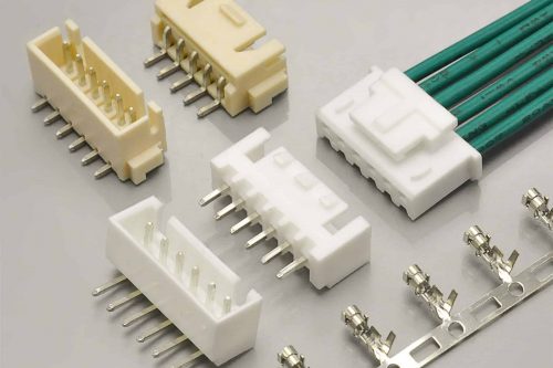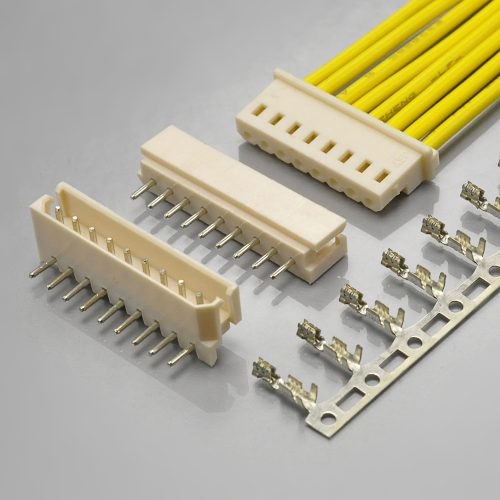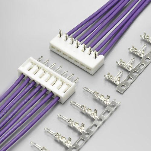
Quick answer: The JST SCN is a 2.5mm pitch, board-in crimp connector — the housing is the part that mounts to the printed circuit board, and the crimped contact is inserted into it from the wire side. There is no separate wafer. JST rates it 3A AC/DC (AWG #22) at 250V AC/DC, over −25℃ to +85℃, with 1,000MΩ minimum insulation resistance, an 800 VAC/minute withstanding voltage, an applicable wire range of AWG #28 to #22, and an insulation window of 0.9mm to 1.7mm. The KONNRA KR2508 is the cross-reference equivalent, and the electrical sheet matches well: the 800V withstand, the 1,000MΩ insulation resistance, the 250V rating and the PA66 UL94 V-0 housing all agree, and the two manufacturers even agree that the contact may be phosphor bronze or brass. Two windows are narrower, and they are the two that matter. The KR2508 documents AWG 24# to 28#, so AWG #22 — the conductor JST references its 3A rating to — has no documented home. And the KR2508 documents 2 to 15 circuits where JST catalogues 2 to 16 — the first time in this series of comparisons that the cross-reference covers less than the original.
What “board-in” Actually Means
Every other 2.5mm family in KONNRA’s range is either wire-to-board (a wafer soldered to the PCB) or wire-to-wire. Board-in is a third architecture, and getting it right is the first thing to do in a cross-reference.
| Board-in (JST SCN pattern) | Wire-to-board (XH, EH, Yeonho 2.5) | Wire-to-wire (JST SM) | |
|---|---|---|---|
| What mounts to the PCB | The housing itself — inserted into board holes | A separate wafer / header | Nothing |
| What carries the wire | The crimped contact, inserted into the housing from the wire side | A crimped contact inside a housing | A crimped contact inside a housing |
| Separate wafer part | None | Required | None |
| Interface construction | 2 parts — board-mounted housing + crimped contact | 3 parts — wafer, housing, contact | 2 housings + 2 contacts |
| Why it exists | Fewest parts, lowest cost, highest density — JST’s own words are “efficiently and economically” | Design flexibility, SMT options, keying | Cable-to-cable joins and panel ports |
The practical consequence is that “board-in” removes a whole component. In a wire-to-board design the bill of materials is a wafer plus a housing plus a contact; in a board-in design it is a housing plus a contact, because the housing is the wafer. That is the economic argument JST makes for the family, and it is the same argument that makes it a good fit for high-volume consumer product.
And it changes what the mating action is. On a board-in connector, assembling the wire side means pushing a crimped contact into a housing that is already on the board — which is why JST’s first listed feature is “Easy inserting contacts into housing” and its second is “Secure mounting on printed circuit boards.” Those two lines are the family’s whole design brief.
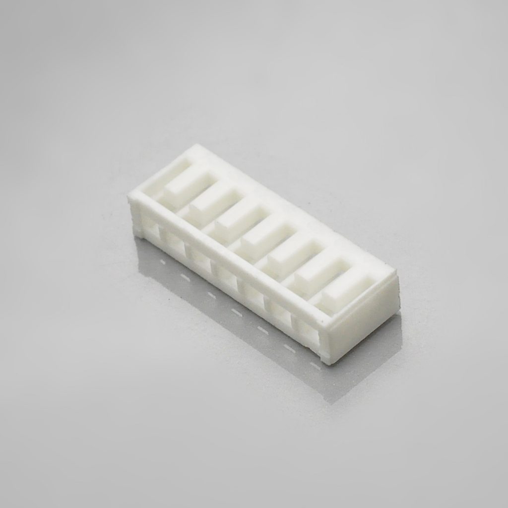
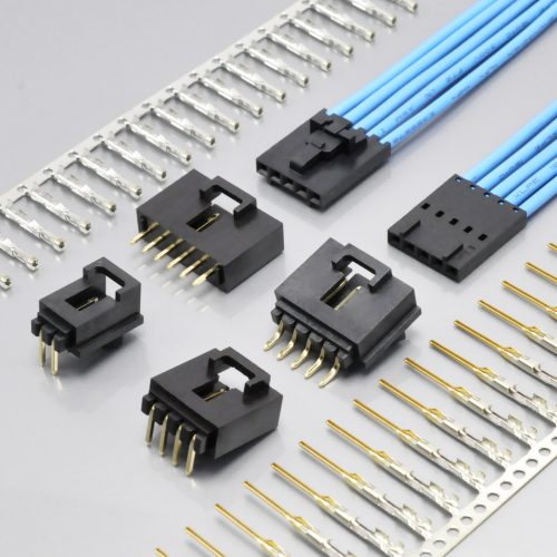
KONNRA KR2508 straight 180 degree board-in housing, mounted to the printed circuit board
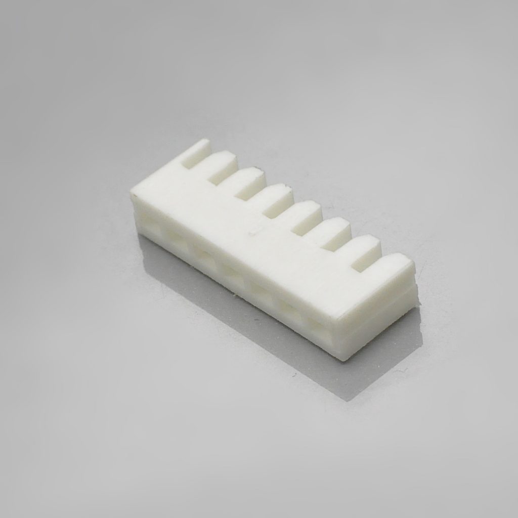
KONNRA KR2508 right-angle 90 degree board-in housing
Two orientation variants exist, and they are separate parts. JST catalogues the housing with a straight and a right-angle body, and the same split runs through the contacts. So a board-in cross-reference is four parts, not two — and, as in the wire-to-wire family, the orientation decides the part number:
| Component | KONNRA part number | Orientation |
|---|---|---|
| Housing, straight | H2508V***0101B |
180° |
| Housing, right-angle | H2508R***0101B |
90° |
| Terminal, straight | T2508VBT0101C |
180° |
| Terminal, right-angle | T2508RPT0101C |
90° |
| Wafer | None | — |
“Wafer: None” is the correct answer, not a gap — there is no separate board-side part in a board-in design. The specification states it explicitly in its part-number table, and then carries the same statement through the material section, where every wafer row (straight and right-angle, base, contact and solder tab) reads “N/A”. That is a documentation decision worth crediting: it is the opposite of the usual failure, where a specification copied from a board connector keeps wafer sections nobody can fill in.
What the JST SCN 2.5 Connector Is
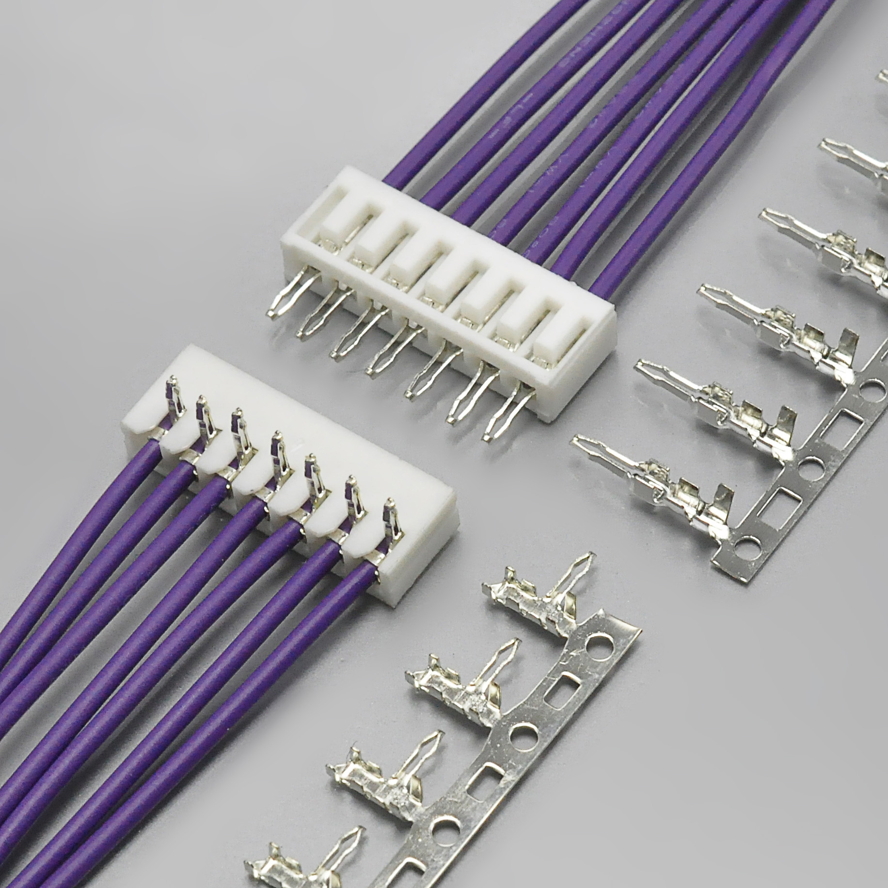
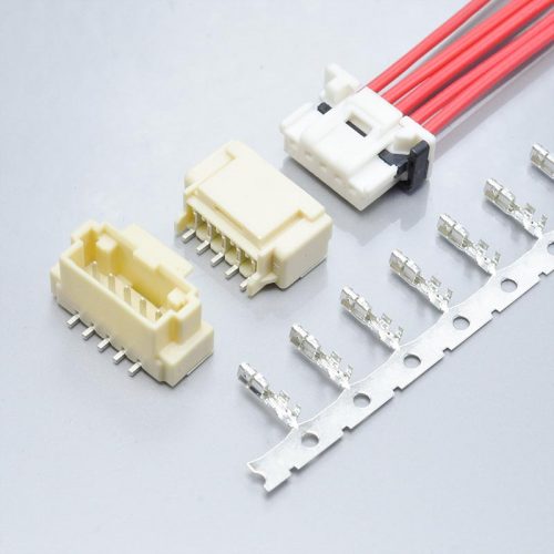
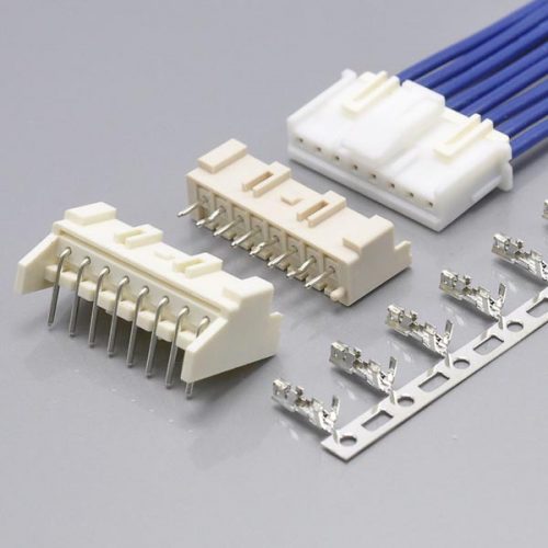
KONNRA KR2508 series SCN 2.5 board-in connector, the cross-reference for the JST SCN 2.5
JST’s own catalogue introduces the family in two sentences, and both are worth reading closely:
“This 2.5 mm pitch multi-circuit board-in connector meets the needs for high-density mounting on printed circuit boards efficiently and economically.”
“The connector can be used for VCRs, car stereo systems, audio products, and many other consumer-oriented electronic products.”
That second sentence is a positioning statement, not a limitation. JST is telling you where the family was designed to win: inside consumer product where board space is tight and the connector count is high. It is the connector you use when you need a reliable 3A connection on a dense board and you are paying for it a hundred thousand times.
JST lists three features:
- “Easy inserting contacts into housing” — the contact is pushed into the board-mounted housing, and JST’s design intent is that this is simple enough for a high-volume assembly line. The KR2508’s page describes the same thing as “users can easily insert contacts into KR2508 series connectors without complicated operations”.
- “Secure mounting on printed circuit boards” — the housing’s own retention in the board is the family’s mechanical anchor, because there is no wafer to hold it.
- “Two types of contacts” — and this is where the family gets interesting, because the two contact types are not simply the two orientations.
The two contact types, and the “K type”
JST publishes two contacts, and the difference between them is material and board thickness:
| JST contact | Material | Applicable board |
|---|---|---|
SCN-001T-P1.0 |
Phosphor bronze | Standard 1.6mm board |
SCN-001T-1.0K |
Brass | K type — 1.6mm and 1.2mm boards |
The K type is the thin-board variant, and JST publishes the board-thickness distinction in both the specification block and the board-layout notes. The catalogue says the applicable PC board thickness is 1.2mm and 1.6mm, and then adds: “Applicable PC board thickness is 1.6 mm, and the one of K type is 1.6 mm and 1.2 mm.” So on a 1.2mm board, the standard contact is not the right part.
And the K type carries two further conditions that a designer needs before laying out a board:
“Contact JST for the hole size of K type 7-circuit or more, since it differs from 1.0 ±0.05 dia.”
“Tolerance for the drilling hole pitch on PCB is ± 0.05 throughout, and shall not be cumulative.”
Read the second one twice, because it is the tighter of the two. A non-cumulative ±0.05mm tolerance across a hole pattern is a demanding drilling requirement — and note that the same non-accumulation rule appears in JST’s EH board notes. It is the kind of line that decides whether a board shop can build the part, and it is the first thing to check when a board-in connector does not seat.
Colour is also a variant axis. JST catalogues the housing in ivory (the default), black, red and yellow, and the K contact is supplied with a black housing option in the part-number allocation table. If a build colour-codes its connectors, that is available on the original side.
And JST publishes the tooling. The crimp machine is the AP-K2N, with applicator MK/SCN-001-10 or crimp applicator MKS-L and dies APLMK SCN001-10. Contacts are supplied 11,000 to a reel, and housings 1,000 to a bag.
Key Specifications at a Glance
| Attribute | JST SCN (manufacturer) | KONNRA KR2508 | Verdict |
|---|---|---|---|
| Pitch | 2.5mm | 2.50mm | Match |
| Architecture | Board-in crimp, housing mounts to the board | Board-in, housing mounts to the board | Match |
| Wafer | None | None | Match |
| Orientation variants | Straight and right-angle | 180° and 90° | Match |
| Current / voltage | 3A AC/DC (AWG #22) / 250V AC/DC | 3A (24AWG) / 250V | Rating matches; reference conductor does not |
| Withstanding voltage | 800 VAC/minute | 800V AC/ minute | Match |
| Insulation resistance | 1,000MΩ min. | 1000MΩ Min | Match |
| Contact resistance | Not published in the SCN catalogue | 10mΩ Max (§5.1); 20mΩ after most conditioning tests; 40mΩ after humidity, thermal shock and salt spray | Original gives nothing to compare |
| Applicable wire | AWG #28 to #22 (0.08–0.33mm²) | AWG 24# to 28# | AWG #22 missing |
| Insulation O.D. | 0.9mm to 1.7mm | 1.60mm(Max.) | Ceiling 0.1mm lower; no floor |
| Temperature range | −25℃ to +85℃ (including temperature rise under load) | −40℃ to +105℃ | Wider by 20℃ / 15℃ |
| Circuits | 2 to 16 (2P-SCN … 16P-SCN) |
2 to 15 | One position short |
| Housing material | PA 66, UL94V-0, ivory | PA66 UL94 V-0, white | Match on the resin and the rating |
| Contact base metal | Phosphor bronze (standard) / brass (K type) | Phosphor bronze or Brass | Match — both allow either |
| Contact plating | Tin-plated (reflow treatment) | Tin plated over nickel | Tin finish on both |
| Applicable PC board thickness | 1.6mm; K type also 1.2mm | Not published | Original only |
| Board hole size | 1.0 ±0.05 dia; K type 7+ circuits differs | Not published | Original only |
| Hole-pitch tolerance | ±0.05, non-cumulative | Not published | Original only |
| Colours | Ivory, black, red, yellow | White | Narrower |
| Tooling published | Machine AP-K2N, applicator MK/SCN-001-10, dies APLMK SCN001-10 |
Crimp dimensions only | Original only |
| Agency | Recognized E60389, RoHS2 | UL E482542 | Partial |
Both columns come from manufacturer documents. Sources are listed at the end.
What Matches Exactly
This is a strong set of agreements, and one of them is unusual enough to lead with.
| Figure | JST SCN | KONNRA KR2508 |
|---|---|---|
| Withstanding voltage | 800 VAC/minute | 800V AC/ minute |
| Insulation resistance | 1,000MΩ min. | 1000MΩ Min |
| Voltage rating | 250V AC/DC | 250V |
| Housing resin and flammability | PA 66, UL94V-0 | PA66 UL94 V-0 |
| Contact base metal | Phosphor bronze, or brass for the K type | Phosphor bronze or Brass |
| Architecture and part count | Board-in, no wafer | Board-in, no wafer |
The first two are the ones that matter most, and they are the pair that cross-references get wrong in opposite directions. The 800V withstand is the original’s figure and the KR2508 matches it on both its product page and its specification §5.3 — which is the correct behaviour, and not universal: the KR2501’s product page puts the rated voltage in the withstand row.
The 1,000MΩ insulation resistance is the important one, because it is genuinely high for this family. JST publishes 1,000MΩ for the SCN, and the KR2508 publishes the same. Note that the neighbouring KONNRA board families and the wire-to-wire family publish different figures — 1.2–1.8mm windows and 500MΩ on the SM — so this is not a number the house template produces by default. The KR2508 carries JST’s figure.
And the flammability rating matches, which is worth stating after the previous round. JST specifies the SCN housing at PA 66, UL94V-0, and the KR2508 specification §3.0 and all four component pages say PA66 UL94 V-0. In the wire-to-wire comparison, the cross-reference was documented at V-2 against the original’s V-0 — a genuine difference. That difference does not exist here.
The base-metal agreement is the unusual one. JST offers the SCN contact in phosphor bronze (standard) and brass (K type), and the KR2508 specification says the terminal may be “Phosphor bronze or Brass, Tin plated over nickel” — an allowance rather than a single callout. Both documents permit either material, which is a closer match than a specification that pins one alloy.
And the architecture matches, which is the agreement that makes the rest usable. No wafer on either side, straight and right-angle orientation variants on both sides, and a housing that is itself the board-mounted part. A cross-reference that got the architecture wrong would not be a cross-reference at all — which is why the next two sections matter.
The Wire Window: AWG #22 Has No Documented Home
This is the sharpest finding of the comparison, and it is worth stating precisely.
| Conductor | JST SCN | KONNRA KR2508 |
|---|---|---|
| AWG #22 | ✅ Accepted (0.33mm²) — and this is the conductor JST rates 3A on | ❌ Not documented |
| AWG #24 | ✅ Accepted | ✅ 24# to 28# |
| AWG #26 | ✅ Accepted | ✅ 24# to 28# |
| AWG #28 | ✅ Accepted (0.08mm²) | ✅ 24# to 28# |
JST’s applicable wire range is AWG #28 to #22. The KR2508 documents 24# to 28# — three sizes, missing the heaviest one.
Why #22 specifically matters. JST’s own specification block reads “Current rating: 3 A AC/DC (AWG #22)” — the family’s headline current rating is referenced to AWG #22. The KR2508’s specification says “Rated Current (Max.) 3A(24AWG)”, referencing the same 3A to a lighter conductor.
So the two documents make the same claim on different wires, and the heavier wire is the one left undocumented:
| JST SCN | KONNRA KR2508 | |
|---|---|---|
| Headline current | 3A | 3A |
| Referenced to | AWG #22 | 24 AWG |
| Is AWG #22 in the documented wire range? | Yes | No |
That is a different situation from a conservative rating. A supplier who rates 3A on a heavier wire than the original is being cautious; a supplier who rates 3A on a lighter wire and does not document the heavier one is leaving a gap. If your harness is on AWG #22 — which is the natural choice at this current and the gauge the original was qualified on — the KR2508 as documented does not cover it.
What to do about it: send us the wire specification. The pattern here is the same as in the JST EH comparison, where the KR2504’s window covered two of the original’s six sizes: the documented window is what the specification states today, and whether a particular wire can be supplied is a question we answer in writing rather than something to infer from a table.
And the same instruction applies to the two heavier gauges by extension — if your design is anywhere near the top of JST’s range, the wire is the first thing to confirm, not the last.
Circuits: One Position Short
This is the first comparison in this series where the cross-reference covers less than the original, and it is worth naming as such.
| Source | Circuits |
|---|---|
| JST SCN catalogue — housing models | 2P-SCN, 3P-SCN, … 16P-SCN |
| JST SCN catalogue — part-number allocation | “No. of circuits: 2 to 16“ |
| KR2508 product page | 2-15pin |
| All four KR2508 component pages | 2P~15P |
| KR2508 specification §2.0 | Housing part numbers H2508V***0101B / H2508R***0101B — count field, no published ceiling |
JST catalogues the SCN from 2 to 16 positions; the KR2508 documents 2 to 15. One position short — and it is a position JST sells, with its own model number.
The KR2508’s own documentation is consistent, which is worth saying: the product page and all four component pages say 15. So this is not the internal disagreement that appeared in the KR2501 and KR2502 comparisons — it is a straightforward coverage gap against the original.
Why the 16-way is worth having a conversation about rather than assuming. JST’s board-layout notes add a condition that is count-dependent:
“Contact JST for the hole size of K type 7-circuit or more, since it differs from 1.0 ±0.05 dia.”
So on the original side, the hole pattern itself changes above a certain circuit count for the K-type contact, and the applicable board thickness interacts with the type. A 16-way board-in connector is therefore not simply a longer version of a 4-way — it sits at the top of a range where the interface geometry is already count-sensitive.
If you need 16 positions, ask. Send the count and the board thickness together, because they are not independent questions on this family. If you are at 15 or below, the question does not arise and the documented range covers you.
The Insulation Window: Lower Ceiling, No Floor
| Source | Applicable wire insulation O.D. |
|---|---|
| JST SCN catalogue (contacts) | 0.9mm to 1.7mm |
| KR2508 specification §4.0 | Insulation O.D. 1.60mm(Max.) |
| KR2508 terminal component pages | Insulation Diameter 1.60mm(MAX) |
| KR2508 housing component pages | (not stated) |
| KR2508 product page, General Specification | 2.50mm — see the note below |
The ceiling is 0.1mm lower than the original’s, and there is no floor at all.
JST publishes a two-sided window of 0.9mm to 1.7mm. The KR2508 publishes 1.60mm maximum — so wire whose insulation measures between 1.6mm and 1.7mm is inside JST’s specification and outside ours, and nothing in the KR2508 documentation states a lower bound, so the 0.9mm end is unaddressed as well.
That combination is narrower than it looks, and it is narrower than the neighbouring comparisons. In the KR2504 comparison the ceilings were the same and only the floor was missing; in the KR2507 comparison the ceiling was 1.6mm against a 1.8mm original. Here both ends are affected at once — a 0.1mm lower ceiling and a 0.9mm missing floor — on a window that only spans 0.8mm in total on the original side. On a narrow window, a 0.1mm shift is a meaningful fraction of the whole range.
And the missing floor sits where the family gets used. JST’s 0.9mm floor pairs with the heaviest gauges, where the insulation wall is thin. The KR2508 applies the same 1.60mm ceiling to all three documented wire sizes, with no lower bound.
This is the parameter that fails quietly. An insulation barrel that is too tight for the wire closes on the insulation instead of gripping the conductor; the joint passes a continuity check, ships, and fails in the field. And on a board-in part there is an extra reason to care: the crimped contact is pushed into a board-mounted housing by an operator, so the wire and its crimp see handling that a pre-assembled housing does not — which puts more load on the insulation crimp, not less.
Measure the actual insulation O.D. of the wire on your harness drawing — not the nominal, not the gauge — and confirm it in writing against the contact you are quoting. Because one end of the published window is missing and the other is 0.1mm tighter than the original’s, the datasheet cannot be your safety net for this parameter.
The product page states the pitch in the insulation row
There is one more thing to say about this window, and it is a defect on our own page rather than a difference between products.
| KONNRA document | Insulation O.D. row |
|---|---|
| Product page, General Specification table | 2.50mm, in a field labelled Insulation O.D |
| Specification §4.0 | Insulation O.D. 1.60mm(Max.) — 1.60mm |
| Terminal component pages | Insulation Diameter 1.60mm(MAX) — 1.60mm |
The product page’s insulation row contains 2.50mm — which is the pitch, not an insulation diameter. Nothing about the part has a 2.50mm insulation window; a wire of that diameter is not in this family’s range at all.
Read it as a field-level error on our side. The specification and the terminal pages both state 1.60mm Max, consistently with each other, and the specification is the controlling document. But a designer scanning the product page will read a number that is three times the specification’s and conclude the connector accepts much heavier wire than it does — which is the permissive direction of error, and therefore the dangerous one. It is on our correction list.
And one more sentence on the same page that should be read carefully. The Overview says the “excellent insulation resistance performance can reach as low as 1000MΩ”. The figure is right and matches the specification; the direction is stated backwards — 1,000MΩ is a floor the part must stay above, not a value it drops to. Read it as 1,000MΩ minimum, which is what §5.2 says.
Temperature: the House Figure, for the Fifth Time
| Source | Temperature range |
|---|---|
| JST SCN catalogue | −25℃ to +85℃, stated as including the temperature rise in applying electrical current |
| KR2508 specification §4.0 | Ambient temperature Range −40~+105 |
| KR2508 component pages | −40℃~105℃ |
The KR2508 documents a range 20℃ wider at the hot end and 15℃ wider at the cold end than the original’s, and it is the same house figure the neighbouring KONNRA series carry.
This is now the fifth original against which the same 20℃ divergence appears — JST XH, Yeonho 2.5, JST EH, JST SM and now JST SCN. Five different originals, four different manufacturers, one gap, always in the same direction. That consistency is evidence about the house rating, not about any of the five parts — and it is exactly why the wider range should be treated as a claim to be supported rather than a specification to be inherited.
The supporting tests exist in the specification, and they are worth requesting by clause: §7.4 heat resistance at 105±2 for 96 hours, §7.5 cold resistance at −40±2 for 96 hours, and §7.8 thermal shock over 5 cycles between −40 and +105. If your application runs above +85℃, ask for the heat-ageing report.
And note what the wider range is not. A wider documented range is not a claim that the part is worse — it is a claim that it is better, and it is unverified. The original’s narrower figure is the one that has been bounded by a manufacturer’s own qualification; ours needs the same treatment before it can be relied on.
Crimping: Two Tables, Because There Are Two Terminals
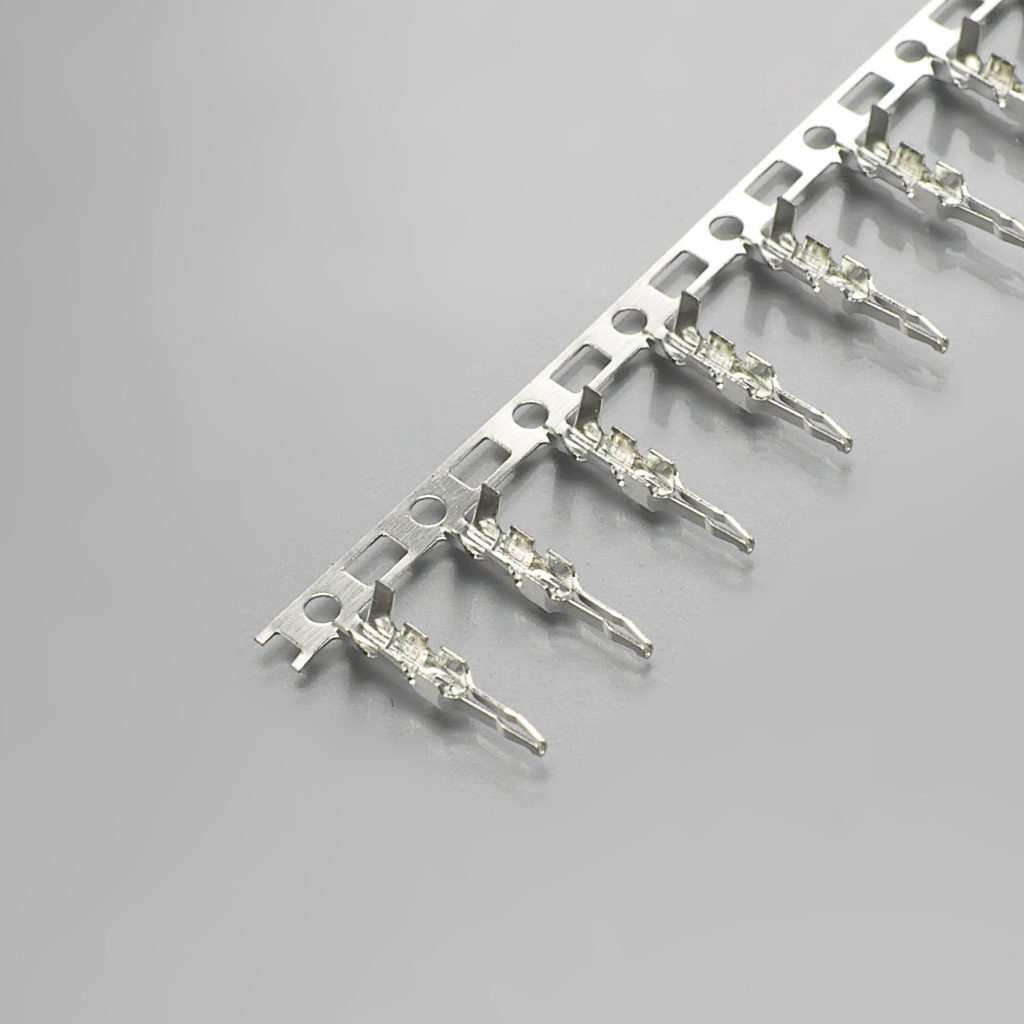
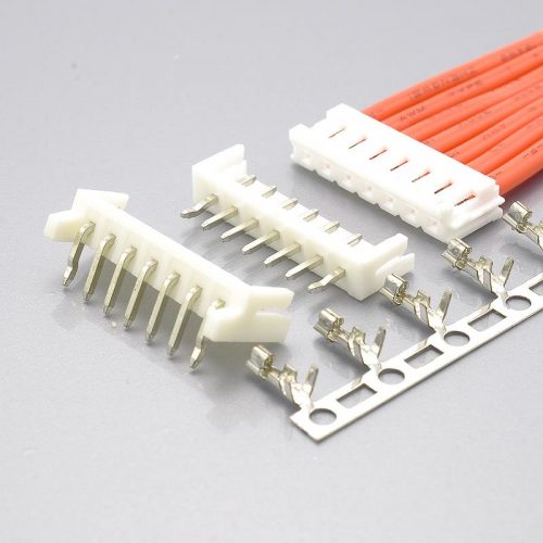
KONNRA KR2508 straight 180 degree crimp terminal for board-in insertion
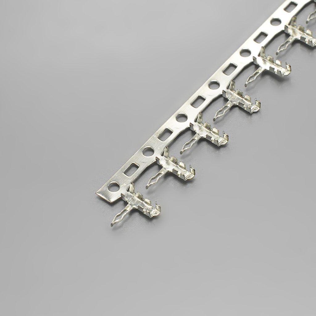
KONNRA KR2508 right-angle 90 degree crimp terminal for board-in insertion
This is where the KR2508 differs from every neighbouring specification in the family, and it is the most operationally important difference.
This specification publishes two crimp tables — §6.3 for the 90° terminal and §6.4 for the 180° terminal. Five previous KONNRA specifications in this range each carried one table, because each had effectively one terminal geometry. This product has two orientations, so it has two.
| Parameter | 24 AWG | 26 AWG | 28 AWG |
|---|---|---|---|
| §6.3 — 90° terminal | |||
| Conductor crimp width | 1.50 ±0.10mm (all three sizes) | ||
| Conductor crimp height | 0.75 ±0.05 | 0.68 ±0.05 | 0.60 ±0.05 |
| Insulation crimp width | 1.80mm max (all three sizes) | ||
| Insulation crimp height | 1.50 ±0.10 | 1.45 ±0.10 | 1.40 ±0.10 |
| Crimp strength | 3.63 kgf min | 2.27 kgf min | 1.36 kgf min |
| Stripping length | 1.3 – 1.8mm (all three sizes) | ||
| §6.4 — 180° terminal | |||
| Conductor crimp width | 1.50 ±0.10mm (all three sizes) | ||
| Conductor crimp height | 0.72 ±0.05 | 0.65 ±0.05 | 0.62 ±0.05 |
| Insulation crimp width | 1.80mm max (all three sizes) | ||
| Insulation crimp height | 1.55 Max | 1.50 Max | 1.40 Max |
| Crimp strength | 3.63 kgf min | 2.27 kgf min | 1.36 kgf min |
| Stripping length | 1.7 – 2.5mm (all three sizes) |
Four things in those two tables matter, and three of them will cost a harness shop a build.
The stripping lengths are different, and this is the one to catch first. The 90° terminal wants 1.3 to 1.8mm; the 180° terminal wants 1.7 to 2.5mm. They overlap only between 1.7mm and 1.8mm — a 0.1mm window — so a setup sheet copied from one orientation to the other will be wrong for essentially every wire, and an operator working from one instruction card will strip to the wrong length on half the orders. This is a place where two very similar-looking parts genuinely need two different process sheets.
The conductor crimp heights differ between the orientations too. 0.75 / 0.68 / 0.60 for the 90° terminal against 0.72 / 0.65 / 0.62 for the 180° terminal. The differences are small — 0.03mm at 24 AWG — but they are specified, which means the dies are not interchangeable.
The two insulation-height columns are given on different bases. The 90° table gives centre plus tolerance (±0.10); the 180° table gives maximums only (1.55 Max, 1.50 Max, 1.40 Max). Both are usable in a setup sheet, but they are not the same kind of number, and a shop that reads the second column as if it were the first will set a nominal that is at the top of the permitted band.
And the crimp strength ladder is identical across both tables — 3.63 / 2.27 / 1.36 kgf minimum for 24 / 26 / 28 AWG. That consistency is a point in the specification’s favour: two different terminal geometries are held to the same mechanical requirement, which is what you would want if the orientation is chosen for board layout rather than for electrical reasons.
One boundary worth checking on your own wire. On the 90° terminal the insulation crimp height at 24 AWG is 1.50 ±0.10mm, so the accepted band runs to 1.60mm — which is exactly the 1.60mm insulation ceiling stated in section 4.0 of the same document. That is a boundary, not an overshoot: the two numbers meet, as they did in the KR2504 comparison. It does mean a 24 AWG wire whose insulation sits at the very top of the range leaves the insulation crimp no closure to work with, so ask for the intended height for that specific wire.
And one gap. KONNRA publishes the crimp geometry but no applicator or crimp-machine part numbers. JST does — machine AP-K2N, applicator MK/SCN-001-10, and dies APLMK SCN001-10 under MKS-L. Note that the original names a single applicator and die set, which suggests one tooling setup covers both SM contacts; whether the same applies to the KR2508’s two terminal orientations is a question for us, and it should be asked with the quote rather than after the first build.
The Mechanical Clauses in PS-KR2508-01
| Clause | What is measured | Test condition | Requirement |
|---|---|---|---|
| §6.1 | Terminal insertion force | Insert the crimped terminal into the housing | 1.0 kgf (9.8 N) max |
| §6.2 | Terminal / housing retention force | Apply axial pull out force at 25.4 ±3mm/minute on the terminal assembled in the housing | 1.5 kgf (14.7 N) min |
| §6.3 | Terminal crimping — 90° terminal | See the crimp table above | Crimp geometry |
| §6.4 | Terminal crimping — 180° terminal | See the crimp table above | Crimp geometry |
Two things are worth noting about this set of clauses.
The retention clause says “pull out”, which is correct and worth confirming. In four of KONNRA’s neighbouring 2.5mm and 2.0mm specifications, the pin-to-pin retention clause instructs the operator to “Apply axial push force” — a retention test that cannot be run as written, because a retention force is the force required to separate two parts and is therefore a pull. In this specification there is no such clause at all: §6.1 is insertion force, §6.2 is retention by pull-out, and §6.3/§6.4 are the two crimp tables. The wording defect is absent from this document — as it was from the KR2507 — which confirms it as a template artefact rather than a universal feature.
And §6.1’s 1.0 kgf maximum is worth relating to the assembly method. The 1.0 kgf cap is the force to push a crimped contact into the housing — and on a board-in connector, that push is a production operation performed by an operator or a machine, not a field mating action. A relatively low insertion force is what you want when the housing is already soldered to a board and someone has to seat dozens of contacts into it, which is precisely what JST means by “Easy inserting contacts into housing”. Both documents agree on this one; it is the same number the KR2501, KR2502 and KR2507 specifications carry.
§6.2 is the clause to design against. A terminal-to-housing retention of 1.5 kgf (14.7 N) minimum means a 1.5kg axial pull on the wire is what the contact must survive inside the board-mounted housing before it moves. That is lower than the 2.0 kgf the neighbouring KONNRA board series specify, and it is the right order for a contact that is pushed in rather than latched by a housing cavity.
Note what is not in this specification, and why. There is no insertion-and-withdrawal force table — no per-circuit-count ladder of mating forces — and there is no §8.0 force table either, because §8.0 in this document is the change-control remark. That is correct for a board-in connector: the crimped contact is pushed into the housing once and left there, so there is no repeated mating action whose force needs to be specified as a function of circuit count. Three of the neighbouring KONNRA specifications carry a 45-figure force table; this one carries none, and the absence is a feature of the architecture rather than a gap.
Environmental and Durability Programme
PS-KR2508-01 §7 publishes a test programme across nine clauses, and it carries three numbering defects that a reviewer should know about before citing it.
| Clause as printed | Test | Condition | Requirement |
|---|---|---|---|
| §7.1 | Temperature rise | Carrying rated current load, EIA-364-70B | Temperature rise 30 max |
| §7.32 | Vibration | Amplitude 1.5mm P-P; sweep 10~55~10 Hz in 1 minute; 2 hours in each X, Y and Z axis, EIA-364-28B | No damage; contact resistance 20mΩ max; discontinuity 1 microsecond max |
| §7.3 | Shock | 490 m/s² (50g), 3 strokes in each axis, EIA-364-27B | No damage; contact resistance 20mΩ max; discontinuity 1 microsecond max |
| §7.4 | Heat resistance | 105 ±2 for 96 hours, EIA-364-17B | No damage; contact resistance 20mΩ max |
| §7.5 | Cold resistance | −40 ±2 for 96 hours, EIA-364-59 | No damage; contact resistance 20mΩ max |
| §7.6 | — | Not present in the document | — |
| §7.7 | Humidity | 40 ±2, 90–95% RH, 96 hours, EIA-364-31B | No damage; contact resistance 40mΩ max; dielectric strength must meet §5.3; insulation resistance 100MΩ min |
| §7.8 | Thermal shock | 5 cycles of −40 for 30 min, room temperature 5 min, +105 for 30 min, room temperature 5 min, EIA-364-32B | No damage; contact resistance 40mΩ max |
| §7.9 | Salt spray | 16 hours at 35 ±2 from a 5 ±1% solution, EIA-364-26B | No damage; contact resistance 40mΩ max |
| §7.10 | Solderability | 3 ±0.5 seconds at 245 ±5, EIA-364-52 | 95% of the immersed area must show no voids or pin holes |
| §7.10 (repeated) | Solder resistance | Soldering time 3~5 seconds, solder temperature 250 max, measured 0.8mm from the terminal tip, EIA-364-71B | No damage |
Three numbering defects, and why they matter to a reviewer
The vibration clause is printed as 7.32. It sits between §7.1 and §7.3, so it is plainly the second clause — but it is printed as 7.32, which reads as a sub-clause of a 7.3 that comes after it. When you write a test procedure against this document, cite the clause by its subject and not only by its number, because the number as printed will not resolve.
Two different clauses are both numbered 7.10 — solderability and solder resistance. They are distinct tests with distinct conditions (a 3-second dip at 245℃ for solderability; a 3-to-5-second exposure at 250℃ maximum, measured 0.8mm from the tip, for solder resistance). A purchase order or a test plan that cites “clause 7.10” is ambiguous, and the ambiguity is inside the document rather than in how it is quoted.
And there is no §7.6. The numbering runs 7.5, 7.7, 7.8, 7.9 — so a reviewer cross-checking the document against a list will find a gap and may assume a clause was lost in a revision. It was not: the programme is complete, with nine tests across ten printed numbers. But the gap is worth knowing about before someone raises it as a finding, because the natural conclusion from a missing clause number is that the document is incomplete.
What the programme actually establishes, once the numbering is set aside, is sound. The conditioning levels are demanding — heat at 105 ±2 for 96 hours, cold at −40 ±2 for 96 hours, thermal shock over five cycles between those temperatures, and vibration for 2 hours in each of three axes with a 1 microsecond maximum discontinuity requirement.
And the contact-resistance limits split into two tiers, as they have throughout this family. Four clauses — vibration, shock, heat and cold — permit 20mΩ; three — humidity, thermal shock and salt spray — permit 40mΩ. Section 5.1 sets 10mΩ max on a dry-circuit measurement, so the document allows the limit to double for the milder conditioning and to quadruple for the three harshest tests. JST publishes no contact-resistance figure for the SCN at all, so unlike the wire-to-wire comparison — where JST’s 10mΩ initial and 20mΩ post-test figures could be compared — there is nothing on the original side to reconcile against. The limits stand on their own.
Humidity is the only test that tightens the insulation-resistance requirement — §7.7 requires 100MΩ min, against the 1,000MΩ min set in §5.2 for a dry part. That is a sensible allowance for absorbed moisture on a PA66 housing, which is a moisture-absorbing polymer, and it is the mechanism behind the change in insertion and withdrawal force that shows up on a humid production floor.
Salt spray runs for 16 hours — a moderate exposure, and the test to revisit if the connector sits in an outdoor or wash-down product. Note that JST’s stated use cases for this family are consumer electronics — VCRs, car stereos, audio products — which is a benign environment, and 16 hours is consistent with that positioning.
The Board Interface: Where the Data Is on One Side Only
For a board-in connector this section is not a detail. The housing is the board-mounted part, so the board layout is the interface, and the original publishes a full set of manufacturing conditions for it.
| Board parameter | JST SCN | KONNRA KR2508 |
|---|---|---|
| Applicable PC board thickness | 1.6mm; K type also 1.2mm | Not published |
| Board hole diameter | 1.0 ±0.05 dia | Not published |
| Hole size for K type, 7 circuits or more | Differs — contact JST | Not published |
| Drilling hole pitch tolerance | ±0.05 throughout, and shall not be cumulative | Not published |
| Which side the layout drawing is viewed from | “The above figure is the figure viewed from the soldering side” | Not published |
| Hole dimensions vs board type and piercing method | “Hole dimensions differ according to the type of PC board and piercing method” — the published dimensions are for reference | Not published |
| Board layout dimensions | Published, including the lance side, and a separate set for Type K | Not published |
Five published conditions on the original side, and none on ours. Each one would cost a board respin if it were wrong, and none of them can be inferred from a connector specification:
- The board thickness is a part-number decision, because the standard contact and the K type are specified for different thicknesses. Get that wrong and the contact does not seat correctly.
- The hole diameter of 1.0 ±0.05mm is a drilling instruction, and the K type’s 7-circuit-and-above exception means the hole pattern changes with the circuit count — so the count and the hole size are not independent choices.
- A non-cumulative ±0.05mm pitch tolerance is tighter than a tolerance that is allowed to accumulate, and it constrains how the panel is drilled. On a 15-way connector the difference between cumulative and non-cumulative is not academic.
- The soldering-side view convention determines whether the board layout is mirrored. It is a one-line note and a whole respin if it is missed.
- And the reference-only caveat on hole dimensions tells you the published numbers are a starting point, and that the board material and the drilling method both move them.
What to do about it. Nothing here is a difference between the two products — it is a difference in what has been published. The KR2508 is a board-in connector with the same architecture and the same 2.5mm pitch, so the interface is physically the same kind of interface; but the board layout, the hole size and the thickness conditions need to come from us as a drawing, not from the product page.
Ask for the board layout drawing for your board thickness and circuit count, together with the four component drawings. It is the same request as the panel cut-out request in the wire-to-wire guide, and it exists for the same reason: on the parts of a connector that touch the customer’s other components, a drawing is the document that settles the question, and a specification is not.
Materials and Colours
| Item | PS-KR2508-01 §3.0 |
KR2508 component / product pages | JST SCN |
|---|---|---|---|
| Housing resin | PA66 UL94 V-0 | PA66 UL94 V-0 | PA 66, UL94V-0 |
| Contact base metal | Phosphor bronze or Brass | — (product page material row lists both) | Phosphor bronze (standard) / Brass (K type) |
| Contact plating | Tin plated over nickel | Tin over Nickel | Tin-plated (reflow treatment) |
| Wafer | N/A — all rows, both orientations | — | No wafer in the architecture |
| Colour | — | White | Ivory (default), black, red, yellow |
The resin callout is a straight answer, and the rating matches the original. The specification and all four component pages say PA66 UL94 V-0, and JST specifies the SCN housing at PA 66, UL94V-0. Two documents, one polymer, one flammability grade, and the grade is the stronger of the two ratings in the V-series. That is worth stating explicitly in this series of guides, because the previous comparison in this family — the wire-to-wire one — found a genuine V-2-against-V-0 difference. It does not occur here.
The base-metal row is the closest match in the whole comparison. JST offers the SCN contact in phosphor bronze as standard and brass on the K type; the KR2508 specification says the terminal may be “Phosphor bronze or Brass, Tin plated over nickel”. Both documents permit either alloy, which means the material row cannot be the source of a discrepancy — and it also means that if your design or your customer’s specification pins one alloy, say which, because both documents allow the other.
Both finishes are tin. JST specifies tin-plated with a reflow treatment; the KR2508 specifies tin over nickel. Both end in tin over a barrier layer, which is the combination that prevents a diffusion layer from growing at temperature. Neither is bare brass or bare copper under the tin.
And one gap worth raising at quotation. JST catalogues the SCN housing in ivory (the default), black, red and yellow, and the part-number allocation table ties the K contact to a black housing option. KONNRA documents White only. If colour coding keeps a 4-way signal cable from being seated into a 4-way power housing on the same board — which is exactly the risk on a dense consumer board — that is a conversation for quotation rather than drawing release.
Documentation and Change Control
PS-KR2508-01 is a 6-page document, Edition A1, carrying the same date in its “Date Issued” and “Date Revised” fields — 2022/2/26 — and no revision history table.
The change-control remark sits at §8.0, not §9.0, and reads:
“Any change or revision for the product specification will not beannounced in advance. Please contact our sales representative for the latest information.”
(The missing space in “beannounced” is in the source document.) The signature block reads “Written: Arvin · Checked: / · Approved: Min xinhao”, with the checking field left empty.
Note the clause numbering, because it differs from the neighbouring specifications. In the KR2501, KR2502 and KR2504 documents the remark is §9.0 after a soldering section; in the KR2507 document it is §9.0 with no soldering section before it; here it is §8.0, because there are two crimp clauses (§6.3 and §6.4) instead of one and no separate soldering section. So the section numbers are not portable between the specifications in this family — cite sections by subject as well as by number.
The drawings are per-component and there are five of them, plus the series drawing and the package specification:
| Document | What it covers |
|---|---|
KR2508-Series-Drawing.pdf |
The series |
KR2508-HV.pdf |
180° / straight housing |
KR2508-HR.pdf |
90° / right-angle housing |
KR2508-TV.pdf |
180° / straight terminal |
KR2508-TR.pdf |
90° / right-angle terminal |
Package-spec_KR2508.pdf |
Packaging |
Five component-orientation drawings is the right documentation for this product, because the four components are genuinely four different parts and a series drawing cannot distinguish a straight housing from a right-angle one. Ask for the drawing that matches the orientation on your board, not only the series drawing.
Against that, here is what the original publishes for the SCN:
- The series catalogue, with the housing model numbers from
2P-SCNto16P-SCN, their A and B dimensions for every count, the quantity per bag, and the material and colour callouts - Contact specifications per part number —
SCN-001T-P1.0and its K type variant — with the applicable wire range, the insulation O.D. window, and the reel quantity - A part-number allocation table that decomposes
SCN-001T-P-1.0and the housing number into series, size, finish, material, shape, circuit count and colour - The full board layout, with the PC board thickness conditions, the hole diameter, the non-cumulative pitch tolerance, the soldering-side viewing convention, the lance side, and a separate layout for the K type
- Crimp machine, applicator and die identifications
- Recognized E60389 and RoHS2 compliance
Two practical consequences.
Quote the revision, not just the series. §8.0 says you will not be told when the document changes, which is common in this industry and is exactly the reason to pin what you designed to. If your qualification file cites the KR2508, cite PS-KR2508-01 Edition A1 and the section number — and, this document being what it is, cite the section by subject too, because two clauses share a number and one number is skipped.
Request the board layout drawing with the quote. This is the one request that belongs in the same email as the price. On a board-in connector the board layout is the interface, and the original publishes five conditions for it that we do not — board thickness, hole diameter, the K-type hole exception above six circuits, the non-cumulative pitch tolerance, and the viewing convention. None of those can be inferred from the connector specification, and each of them costs a board respin if it is wrong.
The 2.5mm Family: Where the KR2508 Sits
Five KONNRA 2.5mm cross-references now exist, and they split into three architectures. This table is the fastest way to see why the choice is structural.
| Attribute | KR2508 — JST SCN | KR2507 — JST SM | KR2504 — JST EH | KR2501 — JST XH | KR2502 — Yeonho 2.5 |
|---|---|---|---|---|---|
| Architecture | Board-in | Wire-to-wire | Wire-to-board | Wire-to-board | Wire-to-board |
| What mounts to the board | The housing | Nothing | A wafer | A wafer | A wafer |
| Separate wafer | None | None | Yes | Yes | Yes |
| Panel mounting | No | Yes | No | No | No |
| Soldering | Housing into board holes | None | Wave | Wave and reflow | Wave and reflow |
| Withstanding voltage | 800 VAC | 1,500 VAC | 800 VAC | 1,000 VAC | 1,000 VAC |
| Insulation resistance | 1,000MΩ | 500MΩ | 1,000MΩ | 1,000MΩ | 1,000MΩ |
| Contact resistance (documented) | 10mΩ | 10mΩ | 20mΩ | 20mΩ | 20mΩ |
| Current / voltage | 3A / 250V | 3A / 250V | 3A / 250V | 3A / 250V | 3A / 250V |
| Wire range (original → KONNRA) | #28–#22 → 24#–28# | #28–#22 → 22#–28# | #32–#22 → 22#–24# | #30–#22 → 22#–28# | #22–#28 → 22#–28# |
| Circuits (original → KONNRA) | 2–16 → 2–15 | 2–12 and 18 → 2–16 | 2–15 → 2–16 | 1–16 and 20 → 2–16 | 2–15/16 → 2–20 |
| Housing flammability | V-0 | V-2 | V-0 | V-0 | V-0 |
Three readings of that table.
The KR2508 is the only board-in cross-reference, and that is a structural position rather than a preference. It has the fewest parts of any family here — a housing that does the wafer’s job and a contact — and it places the housing on the board. If the design needs a panel-mounted connection, this is the wrong family and the SM pattern is the right one. If the design needs a surface-mount or a reflow-processed connector, this is the wrong family too, because a board-in housing goes into drilled holes.
Its electrical position is the same as the EH’s, with a different construction. Both are specified at 800 VAC of withstand — the two lowest in the table — and both are 1,000MΩ. The difference between them is where the contact lives, not what it can carry.
And its wire window is the narrowest documented in the table at the top end. The KR2508’s 24#–28# stops at 24 AWG, where the KR2502 and KR2507 reach 22#, the KR2501 reaches 28#, and the KR2504 reaches 24#. Two of the five cross-references document AWG #22, and this one does not — which matters because JST rates the SCN’s 3A on AWG #22.
Where the KR2508 is the clear choice:
- The design is a dense, high-volume board where the part count and the assembly cost drive the decision
- The board has drilled through-holes and no room for a separate wafer footprint
- The connector is not going to be re-mated in the field — the contact is pushed in once
- AWG #24, #26 or #28 is the wire on the harness
- 2 to 15 circuits covers the design
Where a different family is the answer: the harness is on AWG #22; the design needs 16 positions; the connection has to pass through a panel (SM / KR2507); the design needs surface mount or reflow (XH / KR2501); or the harness is on fine wire, #30 or smaller (EH / KR2504).
➡️ JST SM 2.5 Connector Complete Guide (KR2507) · JST EH 2.5 Connector Complete Guide (KR2504) · JST XH 2.5 Connector Complete Guide (KR2501) · Yeonho YH 2.5 Connector Complete Guide (KR2502) · Explore the full 2.5mm pitch range · Board-in connector range
Further reading on this family: Understanding Board-in Connectors explains the architecture in general terms, and Environmental Testing of SCN Connectors covers what the test programme in this guide is for.
Applications Where the SCN Pattern Is Used
The SCN’s combination — board-in architecture, 2.5mm pitch, 3A, fewest parts — puts it in a specific place in a design: the connector you use when the board is dense and the volume is high.
JST names the family’s intended markets directly: VCRs, car stereo systems, audio products, and many other consumer-oriented electronic products. That framing is about board density and cost rather than about the environment, and it is worth taking at face value when you decide whether the family suits your product.
| Application | Why the SCN pattern fits |
|---|---|
| Audio and home entertainment equipment | JST’s named use case — dense boards, many connectors, moderate current |
| Car stereo and in-vehicle head units | 3A at 250V with a compact board footprint inside a dashboard unit |
| Small appliances and white goods control boards | Multi-way harness connections where the wafer footprint is the constraint |
| Power supplies, adapters and chargers | Board-in housings reduce the component count on high-volume boards |
| Instrumentation and control boards | Dense multi-way I/O where a separate wafer would cost layout area |
| Energy storage and battery management boards | KONNRA’s Overview positions the series at “new energy storage” — a modern use for a board-in layout where a BMS board carries many small-current sense and balance connections |
The honest limits are the wire, the count and the mating. 3A per contact is the ceiling at this pitch. The documented wire window is 24# to 28#, so AWG #22 needs a question before a design commit. The documented count tops out at 15, where JST catalogues 16. And the contact is inserted once and left in place — this is not a family for a connector that gets unplugged in the field, because the assembly action is a push into a board-mounted housing rather than a latch between two housings.
Cable assembly options
Because the board-in housing stays on the customer’s board, the harness KONNRA supplies is the wire side: contacts crimped to cable, supplied loose on reels, in loose-piece quantities, or as a made-up assembly.
| Option | Description | Typical use |
|---|---|---|
| Loose crimped contacts | Contacts crimped to wire, supplied ready to insert into the customer’s board-mounted housings | The standard high-volume pattern — the customer assembles on their own line |
| Single-ended harness | Contacts crimped on one end, bare leads on the other | Where one end lands in a terminal block or a splice |
| Both orientations in one kit | 180° and 90° contacts crimped to length and bagged by orientation | Builds that use both orientations on one board |
| Adapter and transition cables | Board-in contact on one end, another series on the other — to JST XH, to JST PH, to 2.54mm | Interfacing a board-in header to a different board or module |
Two things to specify on any order for this family. First, the orientation — the 180° and 90° contacts are different part numbers with different crimp tables and different stripping lengths, so a mixed order has to be identified by orientation rather than by quantity alone. Second, whether you want loose contacts or a made-up harness, because the standard pattern for a board-in connector is loose crimped contacts supplied to the customer’s line and not a finished cable.
Connector lead time is typically 2–3 weeks; wiring harness lead time is typically 3–4 weeks.
➡️ Explore KONNRA wiring harness capabilities
Sourcing: What Procurement Teams Ask
Engineering decides that a connector will work. Procurement decides whether the supply chain around it is safe — and this family has one question that belongs at the front of the queue.
“Our drawing says SCN or 2P-SCN. Can you supply it?” Yes. Send the full JST part number — a housing (4P-SCN, or the per-circuit model numbers up to 16P-SCN) and a contact (SCN-001T-P1.0, or the K type where a 1.2mm board is involved) — and we will map it to the KR2508 for your circuit count and orientation. Note that JST’s housing number encodes the colour as well as the count, so quote the full string.
“Can you be a second source without changing our design?” On the electrical sheet, yes — and several rows match well: the 800V withstanding voltage, the 1,000MΩ insulation resistance, the 250V rating, the PA66 UL94 V-0 housing and the phosphor bronze or brass contact all agree with the original. Two windows need answering rather than assuming, and they are the ones we would put in writing:
- The wire. JST accepts AWG #28 to #22; we document 24# to 28#. AWG #22 is the conductor JST rates the family’s 3A on, so if your harness uses it, that is the first question.
- The circuit count. JST catalogues 2 to 16; we document 2 to 15. If your design is a 16-way, ask before you commit the layout.
Plus one drawing request: the board layout — thickness conditions, hole diameter, and the pitch tolerance.
“What are your lead times?” Connector production lead time is typically 2–3 weeks; wiring harness lead time is typically 3–4 weeks. Key materials are prestocked to shorten cycles.
“How long for samples?” Complete connector set samples can be delivered within 45 days. For a board-in family, say whether you want loose crimped contacts by orientation or a made-up assembly, because the standard supply pattern is the former.
“What qualifications do you hold?” KONNRA holds ISO9001, ISO14001, IATF16949, ISO45001:2018 and ISO13485 among its quality systems, together with UL product and operational safety certification — the KR2508 components carry UL file E482542. Note that JST lists Recognized E60389 and RoHS2 compliance for the SCN. RoHS is a document request rather than a redesign; raise it at enquiry stage.
“Are you a manufacturer or a trader?” A manufacturer. Dongguan Konnra Electronics Co., Ltd., founded 2004, with in-house mould design, injection moulding, stamping, assembly and inspection — which is why the housing, the contact and the cable assembly can come from one quality system.
“What is the insulation diameter?” 1.60mm maximum, per specification §4.0 and the terminal component pages. Our product page’s General Specification row states 2.50mm in that field, which is the pitch rather than an insulation diameter — it is a field error and it is on our correction list. Work from the specification: 1.60mm Max with no published lower bound, against JST’s 0.9mm to 1.7mm.
How to Get a Cross-Reference Check on Your Part Number
Send us:
- The full JST part number, if you have it — a housing such as
4P-SCNor a per-circuit model number, and a contact (SCN-001T-P1.0for phosphor bronze,SCN-001T-1.0Kfor the K type). Quote the whole string; JST’s housing number encodes the colour as well as the count - The orientation you need — straight or right-angle — and whether the board uses both
- Circuit count, and note that we document 2 to 15 against JST’s 2 to 16
- Wire specification — AWG size and insulation outside diameter measured. The gauge and the insulation window are two different questions on this family, and we are narrower on both
- Your PCB thickness — 1.6mm, or a thinner board. It is a part-number decision on the original side, because the K type is specified for 1.2mm boards
- Any colour-coding requirement — JST offers ivory, black, red and yellow; we document white
- Application and annual volume, so configuration, tooling and packaging can be matched
- A drawing or a photograph, if the part number is unreadable
- Whether you want loose crimped contacts or a made-up cable assembly
What you get back: a mapped KONNRA part number with the relevant drawings including the board layout and the orientation-specific product drawings, a specification comparison against your original part including the wire and insulation windows and the circuit count, written answers on the 16-way and AWG #22 questions, and a sample and quote plan.
Engineer’s Pre-Release Checklist
Run this before you release a drawing for a JST SCN 2.5 pattern connector.
- Confirm the architecture is board-in. The housing mounts to the board and the contact is pushed into it. If the design needs a separate wafer, this is the wrong family.
- Wire gauge checked against the documented 24# to 28#. If the harness uses AWG #22, stop and ask — #22 is the conductor JST rates the 3A on and it is not documented here.
- Insulation outside diameter measured, not assumed, against the 1.60mm Max ceiling. The window has no published floor, against JST’s 0.9mm.
- Ignored the 2.50mm insulation figure on our product page. It is the pitch in the wrong field; the specification says 1.60mm Max.
- Circuit count checked. Documented 2 to 15; JST catalogues 2 to 16. A 16-way needs a question before the layout is committed.
- Orientation decided per position on the board, and the housing and contact orientations matched — 180° housing with the 180° contact, 90° with 90°.
- Two crimp setup sheets written, not one. The 90° terminal strips to 1.3–1.8mm and the 180° terminal to 1.7–2.5mm; the conductor crimp heights also differ. A single setup sheet will be wrong for one of them.
- The 180° terminal’s insulation crimp heights read as maximums, not as centre-plus-tolerance.
- Board thickness confirmed — 1.6mm, or a thinner board, which on the original side changes the contact type.
- Board layout drawing requested. Hole diameter 1.0 ±0.05, non-cumulative pitch tolerance ±0.05, and the soldering-side view convention are published by JST and must come from us as a drawing.
- Board hole pattern checked for the K-type exception above six circuits, if a thin-board variant is involved.
- Temperature requirement checked. Above +85℃, ask for the heat-ageing evidence rather than inheriting the documented −40℃ to +105℃.
- Contact-resistance budget set from the specification: 10mΩ initial, 20mΩ after most conditioning, 40mΩ after humidity, thermal shock and salt spray. JST publishes no figure to compare against.
- Housing colour requirement raised at quotation if colour coding is part of the assembly’s error-proofing — we document white.
- Crimp applicator data requested with the quote. We publish the crimp geometry but no applicator or die numbers; JST publishes
AP-K2N,MK/SCN-001-10andAPLMK SCN001-10. - Accepted that the contact is inserted once. This is not a family for a field-re-mated connection; if the connector gets unplugged, use the panel-mount or board families.
- Test clauses cited by subject as well as number. Two clauses in the specification share the number 7.10, one number (7.6) is skipped, and the vibration clause is printed as 7.32.
➡️ Send us your drawing. We will review it against the KR2508 specification and come back with any mismatch we find — before you commit tooling or a board respin. Submit a drawing for review
Frequently Asked Questions
What is a JST SCN connector?
A 2.5mm pitch, multi-circuit, board-in crimp connector. JST describes it as meeting “the needs for high-density mounting on printed circuit boards efficiently and economically”, and positions it for VCRs, car stereo systems, audio products and other consumer-oriented electronic products. It is rated 3A AC/DC (AWG #22) at 250V AC/DC, over −25℃ to +85℃, with 1,000MΩ minimum insulation resistance, an 800 VAC/minute withstanding voltage, an applicable wire range of AWG #28 to #22, and an insulation window of 0.9mm to 1.7mm.
What does “board-in” mean?
The connector housing is the part that mounts to the printed circuit board, and the crimped contact is inserted into it from the wire side. There is no separate wafer. That makes the bill of materials two parts instead of three — a housing and a contact — which is the cost and density argument JST makes for the family. JST’s two headline features are “Easy inserting contacts into housing” and “Secure mounting on printed circuit boards”, and those two lines describe the whole assembly method.
What is the KONNRA equivalent of the JST SCN 2.5?
The KONNRA KR2508 series — a 2.50mm pitch board-in connector offered as a straight 180° housing, a right-angle 90° housing, a straight 180° terminal and a right-angle 90° terminal, with no wafer. Housing H2508V***0101B (straight) and H2508R***0101B (right-angle); terminals T2508VBT0101C (straight) and T2508RPT0101C (right-angle). All four component pages carry Compatible: SCN Series and are categorised as Board In.
Is the KR2508 a drop-in replacement for the JST SCN 2.5?
On most of the electrical sheet, yes. The 800V withstanding voltage, the 1,000MΩ insulation resistance, the 250V rating, the PA66 UL94 V-0 housing and the phosphor bronze or brass contact all match the original. Two windows are narrower: the KR2508 documents AWG 24# to 28# where JST accepts #28 to #22 — so AWG #22, the conductor JST rates 3A on, is not documented — and it documents 2 to 15 circuits where JST catalogues 2 to 16. The insulation window is also narrower: 1.60mm Max with no floor, against JST’s 0.9mm to 1.7mm.
What wire gauge does the JST SCN accept?
AWG #28 to #22 (0.08mm² to 0.33mm²), with an insulation outside diameter of 0.9mm to 1.7mm, on both the standard contact SCN-001T-P1.0 and the K-type contact SCN-001T-1.0K. The KR2508 documents AWG 24# to 28# with insulation up to 1.60mm — so it omits AWG #22 and applies a 0.1mm lower insulation ceiling, and it publishes no lower insulation bound. Note that the gauge and the insulation diameter are two separate questions here, and we are narrower on both.
What is the current and voltage rating of the JST SCN?
3A AC/DC at 250V AC/DC, and JST references the current rating to AWG #22. The KR2508 documents the same 3A and 250V, but references the current to 24 AWG. That combination is worth reading carefully: JST’s 3A is qualified on a conductor the KR2508 does not document, so if you are running the connector near 3A on AWG #22, ask us for the wire-window answer and the temperature-rise result at that conductor.
What is the withstanding voltage and insulation resistance of the JST SCN?
Withstanding voltage: 800 VAC/minute. Insulation resistance: 1,000MΩ minimum, measured by applying 500V DC for one minute (EIA-364-21B). The KR2508 matches both — its specification §5.3 requires 800V AC for one minute and §5.2 requires 1,000 Megohms Min, and all four component pages state 1000MΩ Min. The 800V figure is one of the two lowest in the 2.5mm family, and it is the original’s figure rather than a limitation the cross-reference introduced.
What is the contact resistance of the JST SCN?
JST does not publish a contact-resistance figure for the SCN — the catalogue’s specification block gives current, voltage, temperature, insulation resistance, withstanding voltage, wire range and board thickness, but no contact-resistance limit. So there is nothing on the original side to compare against. The KR2508 specification §5.1 states 10 milliohms Max on a dry-circuit measurement at 20mV and 100mA maximum (EIA-364-23C); §7 permits 20mΩ after vibration, shock, heat and cold, and 40mΩ after humidity, thermal shock and salt spray. Note that our product page’s Overview prose says “excellent insulation resistance performance can reach as low as 1000MΩ” — the figure is right but the direction is stated backwards; read it as 1,000MΩ minimum.
How many circuits does the JST SCN come in?
2 to 16. JST’s housing models run 2P-SCN through 16P-SCN, and the part-number allocation table states “No. of circuits: 2 to 16”. The KONNRA KR2508 documents 2 to 15 — one position short, and consistently across the product page and all four component pages. If you need a 16-way, ask before you commit the layout.
What board thickness does the JST SCN need?
1.6mm as standard, and the K-type contact also covers 1.2mm. JST’s catalogue states an applicable PC board thickness of 1.2mm and 1.6mm, and adds that the standard thickness is 1.6mm while “the one of K type is 1.6 mm and 1.2 mm” — so a thin board is a contact-type decision, not just a mechanical one. JST also notes that for the K type with 7 circuits or more the hole size differs from 1.0 ±0.05 dia, and that the drilling hole pitch tolerance is ±0.05 throughout and shall not be cumulative. The KR2508 documentation does not publish any of these, so ask us for the board layout drawing.
Which contact do I need — SCN-001T-P1.0 or the K type?
SCN-001T-P1.0 is the standard contact, in phosphor bronze, for a 1.6mm board. SCN-001T-1.0K is the K type, in brass, and it covers both 1.6mm and 1.2mm boards — with a different hole size above six circuits. JST also notes “Contact JST for brass products” on the contact table, and the KR2508 specification allows the terminal to be “Phosphor bronze or Brass”. So if your requirement pins one alloy or one board thickness, say which at enquiry.
Does the connector come in different colours?
JST catalogues the housing in ivory (the default), black, red and yellow, and ties the K contact to a black housing option in the part-number allocation. KONNRA documents the KR2508 in White only. If colour coding is part of the assembly’s error-proofing — keeping a signal cable out of a power housing on the same board — raise it at quotation.
Is the JST SCN a wire-to-board connector?
It is a third architecture. A wire-to-board connector uses a wafer soldered to the board plus a wire-side housing. The SCN is board-in: the housing itself mounts to the board and the crimped contact is inserted into it, so there is no wafer at all. The KONNRA range covers all three — KR2508 board-in, KR2501 / KR2502 / KR2504 wire-to-board, and KR2507 wire-to-wire — and all of them sit at 2.50mm with the same 3A and 250V headline ratings, so the pitch identifies none of them. The architecture does.
How do I identify which 2.5mm connector I actually have?
Measure the pitch first — 2.50mm is this class, 2.54mm is Molex KK or “DuPont”, 2.00mm is JST PH. Then ask one structural question that settles it faster than any dimension: where does the connector attach? If the housing itself goes into holes in the board and a crimped contact is pushed into it from above, it is board-in → KR2508. If a cable housing mates with a wafer soldered on the board, it is wire-to-board → KR2501, KR2502 or KR2504. If the connector joins two cables or passes through a panel, it is wire-to-wire → KR2507. Four architectures, one pitch — the part number and the mounting method are the only reliable identifiers.
How long does it take to get samples?
KONNRA can deliver complete connector set samples within 45 days. For this family, say whether you want loose crimped contacts by orientation — the standard supply pattern for a board-in connector — or a made-up cable assembly. Connector production lead time is typically 2–3 weeks and wiring harness lead time typically 3–4 weeks.
Start Your Cross-Reference Check
KONNRA supplies the KR2508 series as individual components or as pre-crimped contacts and cable assemblies, with customisation available for application-specific requirements.
- Request a quote — KR2508 pricing, MOQ and configuration options for your circuit count and orientation
- Request a sample — complete connector set samples within 45 days, loose contacts by orientation or made-up
- Request cross-reference verification — confirm KR2508-to-JST-SCN equivalence against your specific part number and wire
- Request the wire-window answer — send the AWG and the measured insulation O.D., and we will confirm in writing. This is the first question for this family, because AWG #22 is not in the documented range
- Request the 16-way answer — if your design is a 16-position connector, ask before the layout is committed
- Request the board layout drawing — hole diameter, thickness conditions and pitch tolerance, for your board and circuit count
- Request drawings — the series drawing, and the orientation-specific housing and terminal drawings
- Request the crimp applicator data — and ask whether one tooling setup covers both terminal orientations
- Request a vendor qualification pack — certificates, test capability summary, RoHS and quality documentation
- Submit a drawing for review — we will flag any specification mismatch before you commit tooling or a board respin
Contact KONNRA Electronics
- Phone: (86)-769-85449875
- Email: info@konnra.com
- Address: No.6 Nanchang South Road, Chijiao, Wangniudun, Dongguan, Guangdong, China
- Contact us
Sources and method. Every figure in this guide is taken from a manufacturer document, and where two manufacturers — or two documents from the same manufacturer — disagree, the difference is stated rather than averaged. JST SCN figures are taken from JST’s published SCN connector catalogue: the family description (“2.5 mm pitch/Board-in Crimp style connectors”; “This 2.5 mm pitch multi-circuit board-in connector meets the needs for high-density mounting on printed circuit boards efficiently and economically”; “The connector can be used for VCRs, car stereo systems, audio products, and many other consumer-oriented electronic products”), the three feature lines (easy inserting contacts into housing; secure mounting on printed circuit boards; two types of contacts), the current rating (3 A AC/DC, AWG #22), voltage rating (250 V AC/DC), temperature range (−25 to +85℃, stated as including temperature rise in applying electrical current), insulation resistance (1,000 MΩ min.), withstanding voltage (800 VAC/minute), applicable wire (AWG #28 to #22, 0.08–0.33 mm²), the contact insulation window (0.9 to 1.7 mm), applicable PC board thickness (1.2 mm, 1.6 mm; K type 1.6 mm and 1.2 mm), the board-layout notes (soldering-side viewing convention; hole size 1.0 ±0.05 dia; K type 7-circuit-or-more hole exception; drilling hole pitch tolerance ±0.05 non-cumulative; hole dimensions differ by board type and piercing method), RoHS2 compliance, Recognized E60389, the housing models 2P-SCN through 16P-SCN with their A and B dimensions and quantity per bag, the housing material and colour callout (PA 66, UL94V-0, ivory), the contact part numbers SCN-001T-P1.0 (phosphor bronze) and SCN-001T-1.0K (brass) with their reel quantity of 11,000, the part-number allocation tables for the contact and housing (including the housing colour options ivory, black, red and yellow), and the crimp machine and applicator identifications (AP-K2N; MK/SCN-001-10; MKS-L with dies APLMK SCN001-10). JST XH, JST EH, JST SM and Yeonho 2.5 figures in the family comparison are from the manufacturers’ own published pages and catalogues and from Yeonho Electronics’ own specification sheets, as set out in full in the linked guides. KONNRA KR2508 figures are from PS-KR2508-01 (Edition A1, dated 2022/2/26, 6 pages) sections 1.0, 2.0, 3.0, 4.0, 5.1–5.3, 6.1–6.4, 7.1–7.10 and 8.0, and from the KR2508 product page and the four KR2508 component pages. Four limitations are stated openly. First, JST publishes no contact-resistance figure and no series-level environmental test programme for the SCN, so the KR2508’s figures in those areas are checked against themselves rather than reconciled against the original. Second, the KR2508’s board layout, hole size and thickness conditions are not published on our side — that is a drawing request, and the guide states it as a gap rather than implying the data exists. Third, the KR2508 specification carries three clause-numbering defects — a vibration clause printed as §7.32, two clauses both numbered §7.10 (solderability and solder resistance), and no §7.6 — which are reproduced in this guide as printed so that a reader citing the document can find them. Fourth, the product page’s General Specification row for “Insulation O.D” states 2.50mm, which is the pitch rather than an insulation diameter; the controlling figure is 1.60mm(Max.) from the specification and the terminal pages, and the discrepancy is flagged in the body of the guide. If a figure here disagrees with the current revision of a manufacturer document, the manufacturer document is right.