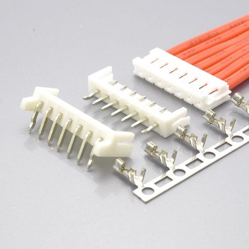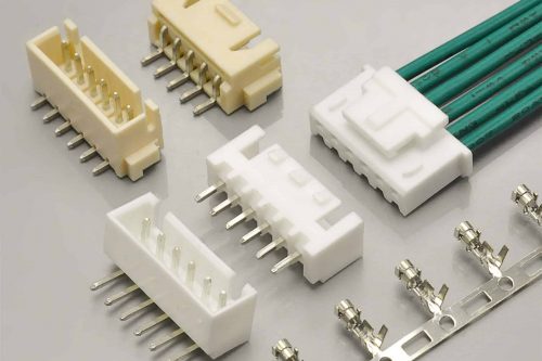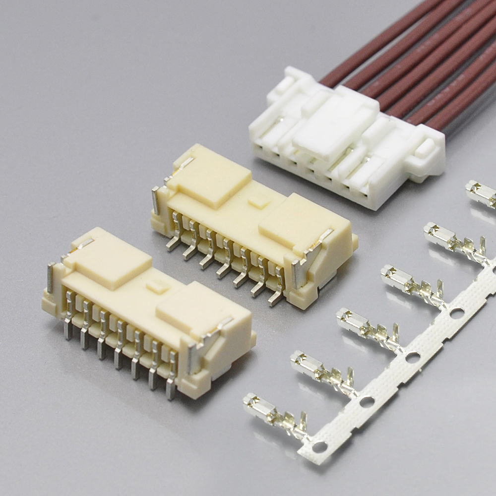
Quick answer: JST’s PAL connector is the wire-to-wire member of JST’s 2.00mm PA family: 2 to 8 circuits, rated 3A AC/DC at AWG #22, 100V AC/DC, −25°C to +85°C, with a conductor window of AWG #28 to #22 and an insulation outside diameter of φ0.9mm to φ1.5mm. The KONNRA KR2022 is the cross-reference offered for it, and it is documented as a wire-to-board set — one housing with a TPA, one terminal and four wafers — specified at 250V, 3A (24AWG) and −40°C to +125°C.
Three things decide whether this replacement works, and each one is visible in the published documents.
The first: the product is titled PAL 2.0, but every part number in its cross-reference belongs to a different JST series. KONNRA’s housing page states Compatible: PARP Series and maps its own part numbers to PARP-02V through PARP-10V; the terminal page states Compatible: SPA Series and maps to SPA-001T-P0.5. In JST’s own catalogue the PAL housing is PALR-02V / PALR-02VF and the PAL contact is SPAL-001T-P0.5 / SPAL-002T-P0.5. None of those PAL numbers appears anywhere on KONNRA’s pages. Section 1 sets the two catalogues side by side.
The second: the wire windows barely overlap. JST’s PAL takes AWG #28 to #22 on insulation of φ0.9mm to φ1.5mm. KONNRA’s specification for the KR2022 takes AWG 20# to 24# on insulation of 1.40 to 1.60mm. The conductor ranges meet at only 22 and 24 AWG; the insulation windows meet only between 1.40 and 1.50mm. A PAL harness built on 26 or 28 AWG wire has no KR2022 coverage at all. Section 2.
The third: the specification’s board-side components are published under KR2014 part numbers. Section 2.0 of PS-KR2022-01 lists the wafers as C2014VD1****M01**PA with three siblings — a 2014 prefix inside a KR2022 document — and the product page’s “Select Components” block displays four KR2014 wafer tiles. Section 4 sets out what that does and does not mean.
One naming note before the table, because it matters more here than on most cross-references. There are three JST 2.00mm retainer-era housing families in the PA system, and they are not interchangeable on paper: PAP-xxV-S (PA connector, standard type), PARP-xxV (PA connector, retainer compatible type) and PALR-xxV / PALR-xxVF (PAL connector, wire-to-wire). Each has its own contact prefix — SPHD-, SPA- and SPAL- respectively — and its own ratings. If you arrived here holding a JST PAL 2.0 part number, confirm which of the three your housing and contact actually are before you read a single number below as applying to you. Section 8 is a three-line test for doing exactly that.
Everything here is taken from KONNRA’s product specification, its product page and its two component pages, and from JST’s own PA-family catalogue and PAL series page, all cited at the end.
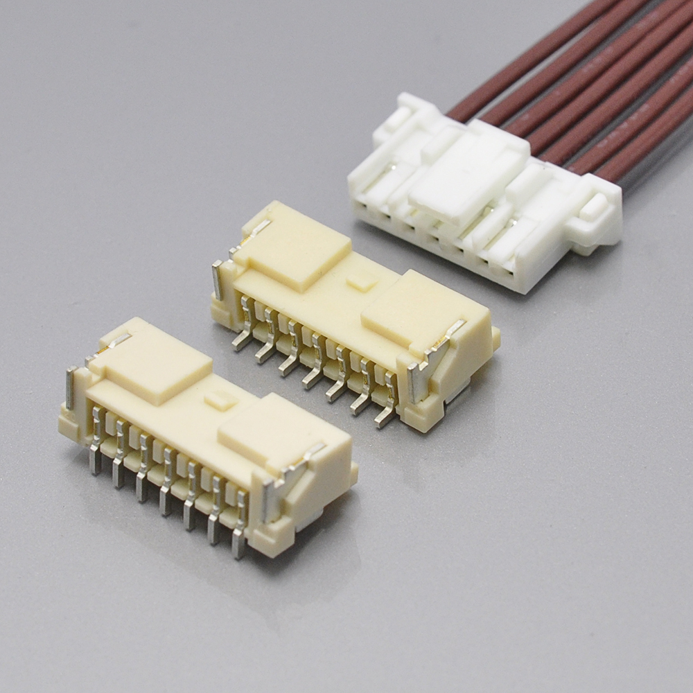
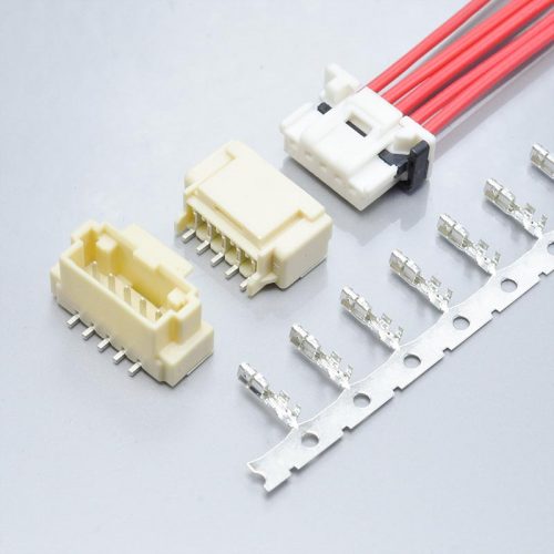
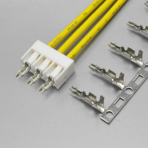
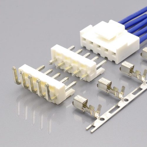
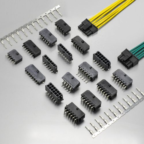
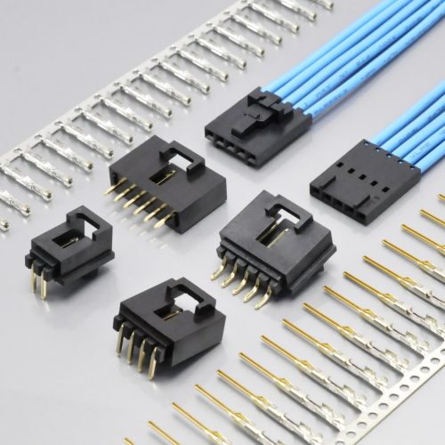
KONNRA KR2022 series PAL 2.0 wire-to-board TPA connector, the cross-reference offered for the JST PAL 2.0 connector
At a glance
| Item | JST PAL 2.0 (wire-to-wire) | JST PARP (PA, retainer-compatible) | KONNRA KR2022 |
|---|---|---|---|
| Family and category | PA family, Wire-to-Wire (JST’s own classification) | PA family, wire-to-board, retainer-compatible type | Documented as Wire to Board on both component pages |
| Pitch | 2.00mm | 2.00mm | 2.00mm |
| Circuits | 2 – 8 | 2 – 13 and 15 (14 absent) | 2-14pin (page) · 2P~15P (housing page) · 2 – 15 (spec force table) · 2 – 10 (cross-reference table) |
| Lock / retention feature | Secure lock (Outer) and Secure lock (Center) | Retainer compatible; retainer available | TPA (housing with TPA published) |
| Rated voltage | 100V AC/DC | 100V AC/DC | 250V (spec §4.0 and all three web pages) |
| Current rating | 3A AC/DC (AWG #22) | 3A AC/DC (AWG #22) | 3A (24AWG) per spec §4.0 · 3A on the pages |
| Operating temperature | −25°C to +85°C | −40°C to +105°C | −40 to +125°C (spec §4.0, component pages) · −40°C to +105°C (product page General Specification) |
| Contact resistance, initial | 15mΩ max | 15mΩ max | 25mΩ max |
| Contact resistance, after test | 25mΩ max | 25mΩ max | 40mΩ max after any conditioning (spec §7.0) |
| Insulation resistance | 1,000MΩ min | 1,000MΩ min | 1,000MΩ min |
| Withstanding voltage | 800VAC for 1 minute | 800VAC for 1 minute | 800V AC for 1 minute (spec §5.3) · “250V AC/minute” (product page) |
| Conductor size | AWG #28 to #22 (0.08 – 0.33mm²) | AWG #26 to #22 (0.13 – 0.33mm²) | AWG 20# to 24# |
| Insulation outside diameter | φ0.9mm to φ1.5mm | φ0.9mm to φ1.5mm | 1.40 to 1.60mm (spec §4.0) · 1.60mm MAX on the pages |
| Panel / board interface | Panel thickness 0.5mm to 2.0mm | PC board thickness 1.6mm | not published |
| Housing part number | PALR-xxV · PALR-xxVF | PARP-xxV, with retainer PMS-xxV-S | H202201**0101A · H202201**2411A |
| Contact part number | SPAL-001T-P0.5 · SPAL-002T-P0.5 | SPA-001T-P0.5 | T20220P*****A — cross-referenced to SPA-001T-P0.5 |
| Housing material | PA, natural | PA, natural (retainer PA (GF), natural) | PA66/PBT, UL94 V-0 (spec) · PA66, UL94V-0, white (housing page) |
| Contact material and plating | Copper alloy, tin-plated | Copper alloy, tin-plated | Phosphor bronze, tin or gold over nickel (spec) · tin over nickel (page) |
| Mating cycles | not stated in the PA-family specification reviewed | not stated in the PA-family specification reviewed | 30 cycles at ≤10 cycles/minute (spec §7.1) |
| Agency | PAL series page states Standard: UL; the catalogue refers registration to a separate list | same | UL/USCAR-2, E482542 / FTS2304250401 — on the web pages only; the specification cites no agency file |
| RoHS | RoHS2 compliance stated for the family | RoHS2 compliance stated for the family | not published |
Four rows in that table need a note before you build on them, and each is covered in its own section below.
The cross-reference row is the whole story of this comparison. A designer holding a genuine PAL design will search for PALR-02V or SPAL-001T-P0.5 and find neither. What the pages give instead is the PARP / PMS / SPA family. That is not necessarily wrong engineering — the PA and PAL connectors intermate, and JST’s own PAL page states “Compatible header available (PA connector)” — but it means the cross-reference is written against a different wire-side system than the one the page title names.
The conductor and insulation rows are the two that will stop a build. They are narrow, they sit at the heavy end of the range, and they are the reason section 2 exists.
The voltage row contains a defect that has nothing to do with JST. KONNRA’s own specification says 800V AC for the dielectric test; its own product page says “250V AC/minute” in the withstanding field. Section 3 sets out why 250V is almost certainly the rated voltage placed in the withstanding field.
The temperature row is the one to resolve in writing. The specification and both component pages say −40°C to +125°C; the product page’s General Specification table says −40°C to +105°C. The 105°C figure is the one that matches JST’s own PA and PARP ratings exactly. The 125°C figure is the wider claim, and it is the number a qualification plan would inherit.
1. The identity problem: the title says PAL, the part numbers say PARP
This is the finding to read first, because it determines which of the numbers elsewhere in this article apply to you.
JST’s 2.00mm PA family contains the parts in the table below. Every part number is from JST’s own PA-family catalogue and its PAL series page.
| JST part family | Prefix | What it is | Housing examples | Contact examples |
|---|---|---|---|---|
| PA connector, standard type | PAP- / SPHD- | Wire-to-board, retainer non-compatible | PAP-02V-S … PAP-16V-S | SPHD-002T-P0.5, SPHD-001T-P0.5 |
| PA connector, retainer compatible type | PARP- / SPA- | Wire-to-board, retainer compatible | PARP-02V … PARP-13V, PARP-15V | SPA-001T-P0.5 |
| PA retainer | PMS- | The retainer itself | PMS-02V-S … PMS-13V-S, PMS-15V-S | — |
| PAL connector | PALR- / SPAL- | Wire-to-wire, panel lock or free-hanging | PALR-02V … PALR-08V · PALR-02VF … PALR-08VF | SPAL-001T-P0.5, SPAL-002T-P0.5 |
Now the same exercise on KONNRA’s side, taken verbatim from its three pages:
| KONNRA source | Statement | JST series it names |
|---|---|---|
| Product page, title | “KR2022 Equivalent To Jst PAL 2.0 Alternatives connector” | PAL |
| Product page, description | “PAP PASK PASS PARP SPA connectors, The 2.0 mm pitch PA family consists of the following connectors: ・PA connector ・PAF connector ・PAL connector” | PARP, SPA, and the PA family generally |
Housing page, Compatible field |
“PARP Series“ | PARP |
| Housing page, cross-reference table | H202201**0101A ↔ PARP-02V … PARP-10V; H202201**2411A ↔ PMS-02V-S … PMS-10V-S |
PARP and PMS |
Terminal page, Compatible field |
“SPA Series“ | SPA |
| Terminal page, cross-reference table | T20220P*****A ↔ SPA-001T-P0.5 |
SPA |
| Terminal page, download link | Product Drawing file is named PAL2.0-Terminal.pdf |
PAL |
So the word “PAL” appears in the product title and in one PDF filename, and nowhere in any part number. Every orderable JST number on the site — housing and contact alike — belongs to the PA retainer-compatible line, which JST classifies as wire-to-board and rates at 100V AC/DC and −40°C to +105°C.
Three consequences follow, and the third is the one to act on.
A PAL design’s own numbers are absent. PALR-02V, PALR-02VF and SPAL-001T-P0.5 are distinct JST catalogue entries with their own wire ranges, and none is listed. If your incoming inspection sheet cites a PAL housing or a SPAL contact, there is no published KONNRA number to check it against.
The two JST systems differ on paper even though they intermate. JST rates the PA retainer-compatible housing at 100V / −40 to +105°C and the PAL housing at 100V / −25 to +85°C. The temperature difference is real: 20°C at the top end and 15°C at the bottom. So “the PA family rating” is not a single figure, and which one applies depends on which housing you hold.
And neither of them is rated at 250V. Both the PAL and the PARP are 100V AC/DC parts in JST’s catalogue; the 250V AC/DC figure belongs to the PA standard type (PAP + SPHD), which is a third housing and a third contact that KONNRA’s pages do not name. As published, KONNRA’s 250V is not traceable to the JST part number its cross-reference gives. That is not automatically wrong — a replacement can exceed the original’s rating — but it is a claim that needs its own test evidence rather than an inherited figure, and it is the first thing to put in writing to the supplier.
The contact part numbers differ by three letters, and the difference is not cosmetic
The terminal cross-reference is worth isolating, because the two JST numbers involved look almost identical:
| JST contact | Belongs to | Conductor | Insulation O.D. | Reel quantity |
|---|---|---|---|---|
| SPA-001T-P0.5 | PA connector, retainer compatible type | #26 to #22 (0.13 – 0.33mm²) | 0.9 to 1.5mm | 10,000 |
| SPAL-001T-P0.5 | PAL connector | #26 to #22 (0.13 – 0.33mm²) | 1.0 to 1.5mm | 10,000 |
| SPAL-002T-P0.5 | PAL connector | #28 to #24 (0.08 – 0.21mm²) | 0.9 to 1.5mm | 10,000 |
KONNRA cross-references T20220P*****A to SPA-001T-P0.5 — the PA retainer-compatible contact. JST’s PAL contacts are the SPAL- parts, and there are two of them, splitting the wire range between #26–#22 and #28–#24. KONNRA’s table lists one contact.
That matters for a simple reason: a PAL harness on 28 AWG uses SPAL-002T-P0.5, and the KONNRA cross-reference has no entry for it. JST’s own PAL line needs two contact part numbers to cover #28–#22; KONNRA’s cross-reference covers the heavier half only, and does so with a PA part number rather than a PAL one.
2. The wire window: the two ranges meet in a 0.10mm strip
This is the most consequential section in the article for anyone actually building a harness, because it is arithmetic rather than judgement.
| Parameter | JST PAL 2.0 | KONNRA KR2022 | Overlap |
|---|---|---|---|
| Conductor size | AWG #28, #26, #24, #22 (0.08 – 0.33mm²) | AWG 20# to 24# | 22 and 24 AWG only |
| Insulation outside diameter | φ0.9mm to φ1.5mm | 1.40mm to 1.60mm | 1.40mm to 1.50mm only |
Two of JST’s four PAL conductor sizes have no KR2022 crimp row. The KR2022 specification’s crimp table publishes three rows — 24, 22 and 20 AWG. JST’s PAL line covers #28, #26, #24 and #22. The two lists share 24 and 22 and nothing else. So:
- a PAL design on 26 AWG or 28 AWG is outside the KR2022’s published wire range entirely, and
- the 20 AWG row in the KR2022 crimp table is eight gauge steps heavier than the lightest wire JST lists for PAL.
Neither of those is a tolerance question. They are two parts with different wire systems.
And the insulation window is narrower and higher than the original’s. JST’s PAL accepts φ0.9 to φ1.5mm insulation; the KR2022’s specification accepts 1.40 to 1.60mm. The windows overlap only between 1.40 and 1.50mm. A wire with 1.20mm insulation — comfortably inside JST’s window — is 0.20mm outside the KR2022’s floor.
Three KONNRA documents state this window differently, and only one of them states the floor at all.
| Source | Insulation diameter published |
|---|---|
| Specification §4.0 | 1.40 to 1.60 mm |
| Product page, General Specification | 1.60mm MAX |
| Terminal component page | 1.60mm (Max) |
The two web pages publish a ceiling without a floor. A designer who reads “1.60mm max” and selects a 1.00mm wire has read a true statement that is not the whole specification. Only §4.0 of the PDF tells you the window starts at 1.40mm. This is the single most likely way for this cross-reference to fail quietly: the wire crimps, the harness looks correct, and the joint is outside the qualified range.
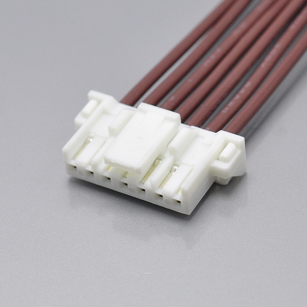
KONNRA KR2022 series 2.00mm pitch housing, the wire-side part governed by the insulation window
The housing page and the terminal page disagree about the wire range too
| Source | Wire range published |
|---|---|
| Specification §4.0 | AWG 20# to 24# |
| Terminal component page | A: 20#-22# B: 22#-24# |
| Housing component page | 22# to 24# |
| Crimp table, specification §6.5 | 24, 22 and 20 AWG rows |
Three of those four include 20 AWG. The housing page does not. Since the housing is the part the wire passes through, and 20 AWG is the heaviest conductor in the range, the one document a buyer would use to check “will my wire fit” excludes the heaviest gauge the rest of the documentation supports.
The terminal page’s two-line split — A: 20#-22# and B: 22#-24# — is worth noting as the most informative of the four, because it implies two terminal grip variants, one for the heavy pair and one for the light pair. No such split appears in the specification’s part-number table, which publishes a single terminal number, T20220P*****A.
3. Voltage, temperature and contact resistance: a reconciliation across five documents
JST’s PA family is not one specification, and KONNRA’s KR2022 is not one specification either. Put every published figure in one grid and three of the cells resolve cleanly while three do not.
| Parameter | JST PA standard | JST PA retainer-compatible | JST PAL | KONNRA spec §4.0 / §5.0 | KONNRA web pages |
|---|---|---|---|---|---|
| Rated voltage | 250V AC/DC | 100V AC/DC | 100V AC/DC | 250V AC/DC | 250V |
| Withstanding voltage | 800VAC, 1 minute | 800VAC, 1 minute | 800VAC, 1 minute | 800V AC, 1 minute | “250V AC/minute” |
| Operating temperature | −40 to +105°C | −40 to +105°C | −25 to +85°C | −40 to +125°C | +125°C on component pages · +105°C in the product page General Specification |
| Contact resistance, initial | 10mΩ max | 15mΩ max | 15mΩ max | 25mΩ max | 25mΩ max |
| Contact resistance, after test | 20mΩ max | 25mΩ max | 25mΩ max | 40mΩ max | not published |
| Insulation resistance | 1,000MΩ min | 1,000MΩ min | 1,000MΩ min | 1,000MΩ min | 1,000MΩ min |
| Current rating | 3A (AWG #22) | 3A (AWG #22) | 3A (AWG #22) | 3A (24AWG) | 3A |
The withstanding voltage is the cleanest defect in the whole comparison
Look at the withstanding row. Three JST figures agree at 800VAC for one minute. KONNRA’s specification agrees at 800V AC for one minute — section 5.3, tested between adjacent terminals or to ground, per EIA-364-20A, acceptance “No Breakdown and Flashover”. The specification and the original match exactly.
Then the product page says “Withstanding Voltage: 250V AC/minute”.
250V is not a withstanding voltage. It is the rated voltage, and it appears elsewhere on the same page in the at-a-glance table as Voltage: 250V. So the row is almost certainly the rated voltage copied into the withstanding field — a failure mode worth naming, because it is the opposite of what happened on another series in this catalogue, where a genuine 500V dielectric figure turned out to be correct and I said so. Here the dielectric figure in the controlling document is 800V, and the page’s 250V is lower than the rated voltage’s own test level.
What to carry forward: 800V AC for one minute, per specification §5.3. And note that the defect runs in the conservative direction, which is the dangerous direction — a designer who needs a 500V withstand will read “250V” on the page and reject a part that is actually specified at 800V.
The temperature: the specification says 125°C, the page says 105°C, and JST says 105°C
| Source | Operating temperature |
|---|---|
| KONNRA specification §4.0 | −40 to +125°C |
| KONNRA housing component page | −40℃~125℃ |
| KONNRA terminal component page | −40℃~125℃ |
| KONNRA product page, General Specification | −40°C to +105°C |
| JST PA standard type | −40 to +105°C |
| JST PA retainer-compatible type | −40 to +105°C |
| JST PAL | −25 to +85°C |
The controlling document and the two component pages agree on −40 to +125°C. The product page is the outlier at +105°C — and +105°C is exactly JST’s figure for the PA and retainer-compatible types.
I am not going to claim the page is right and the specification is wrong, because the opposite is possible: a replacement may genuinely be qualified hotter than the original. But three things are worth putting in front of the supplier.
The specification’s own environmental evidence supports 125°C but not 125°C operation of the whole assembly separately from the wire. Section 7.5 runs 125±2°C for 96 hours as a heat-resistance test, and §7.8 thermal-shock cycles between −40°C and +125°C five times. Those establish that the housing, contact and wafer survive 125°C. They do not establish that a mated connector with a crimped harness runs there — the current rating governs that, and the current rating carries its own limit.
Which is the second point: the governing number is the 30°C temperature rise, not the ambient ceiling. Section 7.2 caps temperature rise at 30°C max when carrying rated current (EIA-364-70B). At a 125°C ambient the connector would be at 155°C before the rise is even counted, which is not what the materials table describes. The usable ambient depends on the current you draw, and JST’s own note says the same thing from the other side: its ratings are quoted “including temperature rise in applying electrical current”.
And the third point is the 3A itself. KONNRA’s specification says 3A (24AWG). JST says 3A AC/DC (AWG #22) on all three of its PA variants. The same current rating is being carried on a thinner conductor here — 24 AWG is roughly 0.205mm² against 22 AWG at roughly 0.326mm², about 37% less copper. Higher current density means more self-heating in the same envelope, and 30°C is the limit that decides whether the claim holds on your harness. This is the bench measurement to make on a first article, not a figure to inherit from either document.
Contact resistance: the specification is 25mΩ initial, which is JST’s after-test figure
| Contact | Initial | After test |
|---|---|---|
| JST PA standard (SPHD-) | 10mΩ max | 20mΩ max |
| JST PA retainer-compatible (SPA-) | 15mΩ max | 25mΩ max |
| JST PAL (SPAL-) | 15mΩ max | 25mΩ max |
| KONNRA KR2022 | 25mΩ max | 40mΩ max |
KONNRA’s specification and its three web pages agree with each other at 25mΩ — there is no internal contradiction on this parameter, which is worth recording given how many other parameters have one. The difference is against the original: KONNRA’s initial limit equals JST’s after-test limit for the SPA and SPAL contacts, and it is 2.5 times the PA standard type’s initial limit of 10mΩ.
On a dry-circuit measurement basis — KONNRA specifies 20mV max, 100mA max per EIA-364-23C, which is the same convention JST’s family uses — those are comparable numbers rather than two different tests. So the honest statement is that this replacement is specified with 1.7× the initial contact resistance of the retainer-compatible original and 2.5× that of the standard type, and it doubles to 40mΩ after any environmental conditioning.
That is not disqualifying for a signal application. It is worth knowing before you compare it against a 10mΩ budget inherited from a PA standard design.
4. The specification publishes KR2014 part numbers for its board-side components
This one is easy to miss and worth checking against your own paperwork.
Section 2.0 of PS-KR2022-01 is the part-number table. It lists four wafers:
| Specification row | Part number as published |
|---|---|
| Wafer, DIP straight | C2014VD1****M01**PA |
| Wafer, DIP right angle | C2014RD1****M01**PA |
| Wafer, SMT right angle | C2014RS1****M01**RA |
| Wafer, SMT straight | C2014VS1****M01**RA |
All four carry a 2014 prefix inside a KR2022 document. The housing and TPA numbers in the same table carry 2022 (H202201**0101A, H202201**2411A) and the terminal carries 2022 (T20220P*****A), so the prefix is not a series-wide convention that happens to read oddly — it is a genuine split inside one table.
Three independent pieces of evidence point the same way:
- The product page’s “Select Components” block shows six tiles. Two are the KR2022 housing and terminal. The other four are KR2014 wafers — the page links to
/components/kr2014-rd-wafer/,/components/kr2014-vs-wafer/,/components/kr2014-rs-wafer/and/components/kr2014-vd-wafer/. - The terminal page’s own drawing file is named
PAL2.0-Terminal.pdf, so the terminal is traced to a PAL 2.0 drawing while the wafers are traced to KR2014 pages. - The same split runs in the other direction on the neighbouring series. The KR2014 DIP straight wafer page links to a KR2022 series drawing.
What this most likely means, and it is an inference rather than something the documents state: KR2022 is a wire-side addition to an existing board-side system. JST’s PA and PAL connectors intermate — its PAL page says so explicitly, “Compatible header available (PA connector)” — so reusing the KR2014 (PA-equivalent) wafer as the board half of a PAL-class housing is coherent engineering. The supporting evidence is that the four wafer part numbers, the four wafer page links and the wafer materials all carry over unchanged.
What it means in practice is narrower and more useful: do not treat a KR2022 wafer as a distinct item. Order it by the C2014... number, and if your drawing already specifies a KR2014 wafer, you may be holding the same part under two article names. That is a purchasing question, not a design one, and it is worth one email.
One thing the split does not do is change the wire-side story: the housing and terminal are published as KR2022 parts with their own numbers, and those are the parts the wire system in section 2 applies to.
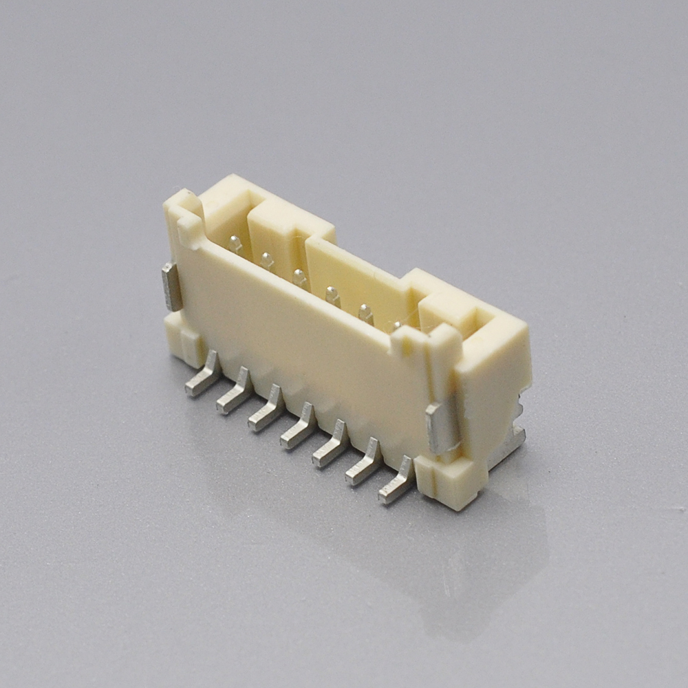
KONNRA KR2022 series straight SMT type wafer, one of the four wafers published under KR2014 part numbers
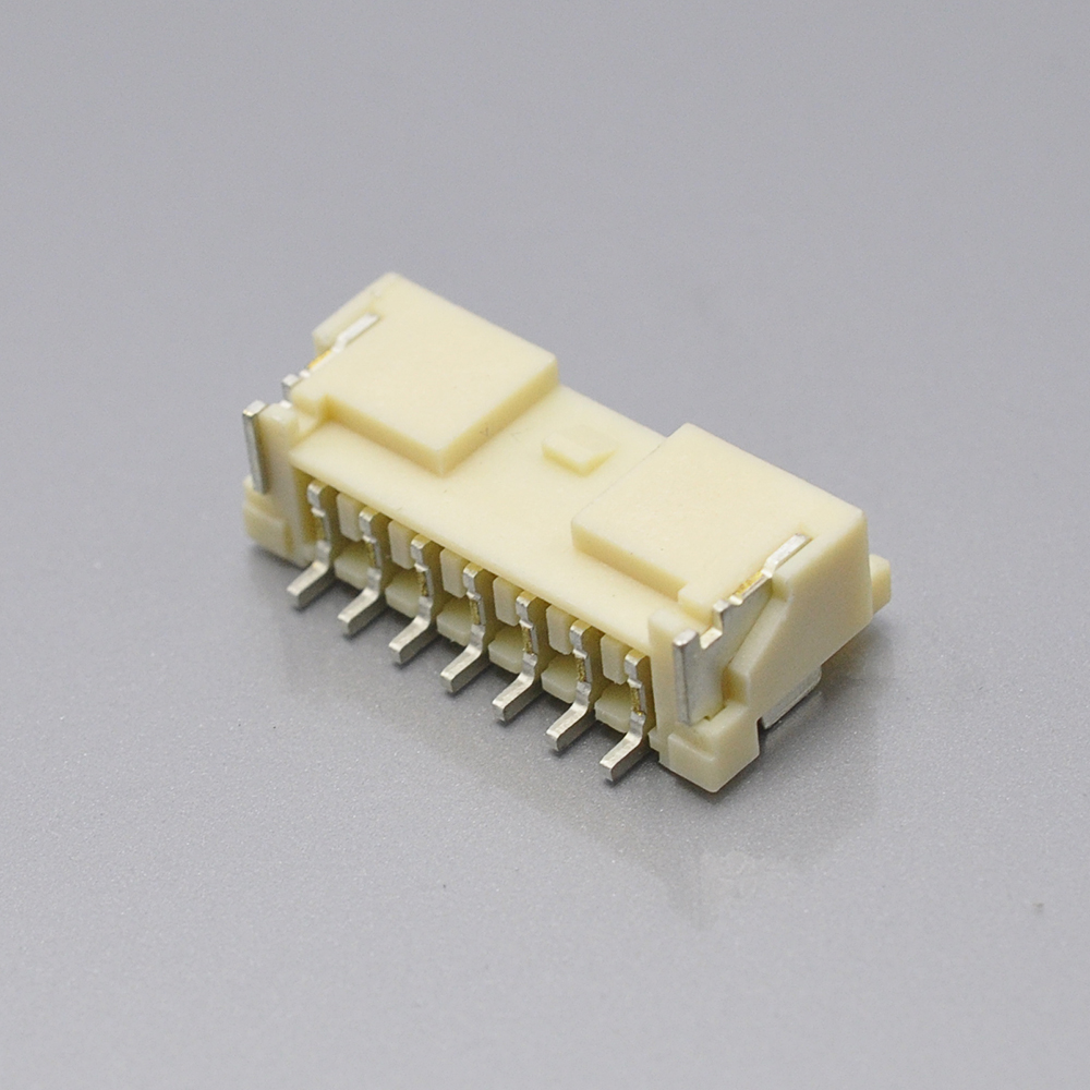
KONNRA KR2022 series right angle SMT type wafer, the second of the four wafers carrying a 2014 prefix
5. The force table: two exact laws, one constant loss, and the same 42 values as KR2014
Section 8.0 publishes insertion and withdrawal force for every circuit count from 2 to 15, at initial and after 30 mating cycles. Units are kgf. The table is printed in two halves in the source; read together it is this:
| Circuits | 2 | 3 | 4 | 5 | 6 | 7 | 8 | 9 | 10 | 11 | 12 | 13 | 14 | 15 |
|---|---|---|---|---|---|---|---|---|---|---|---|---|---|---|
| I.F. max | 1.5 | 2.0 | 2.5 | 3.0 | 3.5 | 4.0 | 4.5 | 5.0 | 5.5 | 6.0 | 6.5 | 7.0 | 7.5 | 8.0 |
| R.F. min, initial | 0.20 | 0.30 | 0.40 | 0.50 | 0.60 | 0.70 | 0.80 | 0.90 | 1.00 | 1.10 | 1.20 | 1.30 | 1.40 | 1.50 |
| R.F. min, after 30 cycles | 0.15 | 0.25 | 0.35 | 0.45 | 0.55 | 0.65 | 0.75 | 0.85 | 0.95 | 1.05 | 1.15 | 1.25 | 1.35 | 1.45 |
Both columns reduce to exact formulas
Insertion force: I.F. = 0.50 + 0.50 × circuits. At two circuits, 0.50 + 1.00 = 1.5. At fifteen, 0.50 + 7.50 = 8.0.
Withdrawal force: R.F. = 0.10 × circuits. At two circuits, 0.20. At fifteen, 1.50.
All twenty-eight published values across those two rows follow the relations with no exception anywhere in the table.
The loss after 30 cycles is a constant absolute 0.05 kgf, at every one of the fourteen sizes — 0.15 against 0.20 at two circuits, 1.45 against 1.50 at fifteen. Because the loss is constant rather than proportional, it costs proportionally more at the small end: 0.05 out of 0.20 is a 25% reduction at two circuits, against barely 3% at fifteen. Both the after-cycles column and the initial column are genuinely different figures rather than one copied from the other, which is the desirable case and not the universal one in this catalogue.
One other constant falls out of the table and is worth having. Withdrawal force is 0.10 per contact; the terminal-to-housing retention in §6.3 is 2.08 kgf (20N) minimum per terminal. Both figures scale with the number of positions, so the ratio between them is fixed at about 21 to 1 at every circuit count — 0.20 kgf of withdrawal against 4.16 kgf of aggregate terminal retention at two circuits, and 1.50 against 31.2 at fifteen. The mating interface is the intended release point, which is the property you want in a connector, and it follows directly from the two published figures rather than being a design claim.
The same 42 values appear in the neighbouring KR2014 specification
The insertion row, the initial withdrawal row and the after-30-cycles row in PS-KR2022-01 are numerically identical, value for value, to the corresponding rows in the KR2014 specification — the same 1.5-to-8.0 insertion ladder, the same 0.20-to-1.50 withdrawal ladder, and the same constant 0.05 kgf loss at every size.
There is a plausible and probably correct explanation, and it connects directly to section 4: if the KR2022’s board-side components are the KR2014’s wafers, the mating interface is the same interface, and its insertion and withdrawal characteristics would legitimately be the same numbers. A shared board half carrying a different wire half should carry the same force table.
But that reasoning only covers the wafer half. The withdrawal force in §8.0 is the force to separate the mated pair, so it depends on the housing’s retention features as much as on the wafer. If the KR2022’s housing and TPA are new parts, an identical force table is an assumption that the new housing reproduces the old one’s contribution exactly.
The practical reading: the table is internally consistent and mathematically clean, so use it. But if your qualification plan treats the force table as measured evidence for the KR2022 specifically, ask whether it was measured on this assembly or carried across from the KR2014 document. It is a fair question and a cheap one, and it decides whether the table is data or inheritance.
6. Crimp data: a ladder that runs in the wrong direction
The crimp table in §6.5 is the one section of this specification I would not quote without checking it against the drawing, and the reason is arithmetic rather than interpretation.
| 24 AWG | 22 AWG | 20 AWG | |
|---|---|---|---|
| Conductor crimp width | 1.25 ± 0.1 | 1.25 ± 0.1 | 1.25 ± 0.1 |
| Conductor crimp height | 0.65 ± 0.05 | 0.74 ± 0.05 | 0.80 ± 0.05 |
| Insulation crimp width | 1.60 Max | 1.60 Max | 1.60 Max |
| Insulation crimp height | 1.55 ± 0.10 | 1.45 ± 0.10 | 1.30 ± 0.10 |
| Crimp strength, min | 4 kgf | 4 kgf | 6 kgf |
| Stripping length | 1.6 – 2.3 mm | 1.6 – 2.3 mm | 1.6 – 2.3 mm |
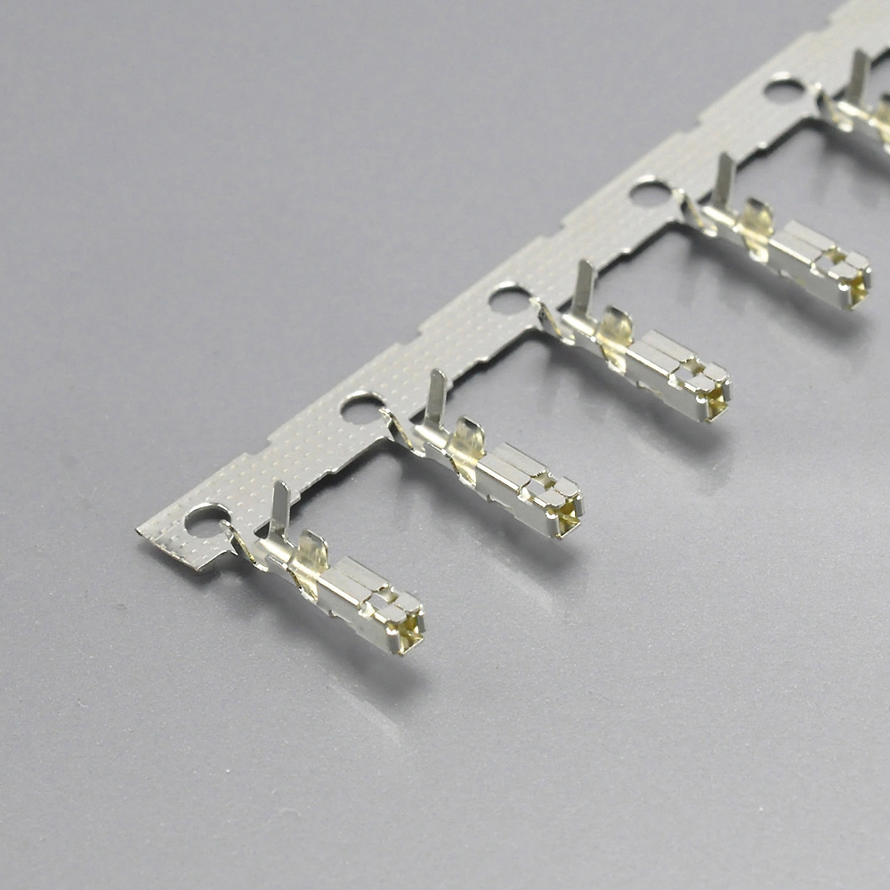
KONNRA KR2022 series 2.00mm pitch terminal, the crimp contact specified in section 6.5
The conductor block behaves correctly. Crimp height rises with conductor size — 0.65mm at 24 AWG, 0.74mm at 22 AWG, 0.80mm at 20 AWG. That is the physically expected direction: a heavier conductor needs a taller crimp. The column order in the source is therefore confirmed by its own data, which matters for reading the row below it.
The insulation block runs the other way. It falls from 1.55mm at 24 AWG to 1.30mm at 20 AWG — the insulation crimp gets smaller as the wire gets thicker. That is the opposite of what an insulation crimp does, because the insulation barrel closes on the wire’s insulation, and thicker wire carries thicker insulation, not thinner.
And the bottom of that ladder contradicts the specification’s own wire window. Section 4.0 permits an insulation outside diameter of 1.40mm minimum. The 20 AWG insulation crimp height is 1.30 ± 0.10mm — so even at the top of its tolerance band the crimp reaches 1.40mm, exactly the smallest insulation the same document allows, and at nominal it sits 0.10mm below the minimum wire it is supposed to accept. A 20 AWG wire in this range cannot pass through a 1.30mm insulation crimp without the barrel crushing the insulation.
The probable origin is visible in the neighbouring series. The KR2014 and KR2021 crimp tables publish the same insulation ladder — 1.55 / 1.45 / 1.30 ± 0.10 — but against wire gauges running 24 / 26 / 28 AWG, where the ladder descends in the correct direction because the wire gets thinner from left to right. The KR2022 table uses the identical three numbers against 24 / 22 / 20 AWG, where the wire gets thicker from left to right. I am flagging this as an observation about the documents rather than as a proven copy error, because the source does not say — but the numbers are identical, the direction is inverted, and the resulting value falls below the specification’s own minimum insulation diameter.
What to do with it: use the conductor row as published, treat the crimp strength row as the acceptance limit (4 / 4 / 6 kgf minimum), and get the insulation crimp height for your actual wire confirmed against the terminal drawing rather than the specification table. The specification itself points the same way — its materials section carries the note “Please Refer to the Project drawing for the above Specification.”
7. Materials and plating, component by component
The product page compresses the whole bill of materials into one row — Material: C5191R PBT PA66 PA9T — which lists one copper grade and three polymers without saying which component uses which. The specification resolves it, and the resolution matters:
| Component | Base material | Plating |
|---|---|---|
| Housing and TPA | PA66 / PBT, UL94 V-0 | — |
| Terminal | Phosphor bronze | Tin or gold over nickel |
| Wafer base, SMT and DIP | PA9T or LCP, UL94 V-0 | — |
| Wafer contact, SMT | Brass | Matte-tin over nickel |
| Wafer contact, DIP | Brass | Matte-tin or gold over nickel |
| Wafer solder tab, SMT | Brass | Matte-tin over nickel |
| Wafer solder tab, DIP | None | None |
Three rows in that table need a note.
Gold is available on the terminal and on the DIP wafer contact — and not on the SMT wafer contact. The specification states “Tin/Gold Plated Over Nickel” for the terminal and “Matte-Tin/Gold Plated Over Nickel” for the DIP wafer contact, but matte-tin only for the SMT wafer contact and its solder tab. So a gold board interface forces the DIP wafer, and a gold wire interface is open on either style.
The web pages hide the gold option entirely. The product page’s General Specification says Product Plating: Tin Plated Over Nickel, with no mention of gold. The terminal page does not state a plating at all. So a designer who needs gold at the wire side will not find it from the pages — only from section 3.0 of the PDF. If your application needs gold, quote it from the specification and confirm it in the RFQ.
The DIP solder tab is “None”, and that is correct rather than missing. A through-hole wafer is held by its own posts passing through the board, so it needs no separate soldered anchor; the SMT wafer is held by solder tabs plus its contacts. Recording an intentional absence as “None” is the right way to document it, because it stops a reader wondering whether the field was left blank.
The housing material is left open by the controlling document
| Source | Housing material |
|---|---|
| KONNRA specification §3.0 | PA66 / PBT |
| KONNRA housing component page | PA66, UL94V-0 |
| JST PA retainer-compatible housing | PA, natural |
| JST PAL housing | PA, natural |
The specification does not decide between PA66 and PBT; the page commits to PA66; JST uses PA. Those are three different answers, and the difference is not academic — PA66 and PBT differ in moisture uptake, in dimensional stability under humidity, and in how they behave through reflow. Get the resin fixed in writing before qualification, and note that the specification’s own materials section carries the instruction “Please Refer to the Project drawing for the above Specification” — the drawing, not the table, is the controlling document for materials.
Plating system: tin over nickel here, tin-plated there
JST’s PA-family catalogue states copper alloy, tin-plated for the SPHD, SPA and SPAL contacts alike — a single-layer callout with no nickel barrier mentioned. KONNRA’s specification specifies phosphor bronze with tin or gold over nickel, so a nickel under-plate on every plated surface including the solder tabs.
Two differences follow. The base alloy differs: phosphor bronze is a different metallurgy from the generic “copper alloy” JST lists, with different spring properties, and it is the more specific callout. And the nickel barrier is an addition, which is the construction that keeps a matte-tin surface stable at elevated temperature — worth having, and worth noting as a difference rather than a match.
Colour is not an option here
KONNRA’s housing page states Color: White and the specification publishes a single housing material, so there is no colour variant. JST’s PA family, by contrast, runs a full colour-code field in its ordering logic — S for natural, K black, R red, E blue, M green, O orange, N brown, P purple, PK pink, Y yellow, L lemon yellow, FY fluorescent yellow, LE light blue, H grey and TR tomato red.
If your assembly procedure uses colour to prevent cross-mating, this series does not support that method, and the mating-key geometry is what you will have to rely on instead.
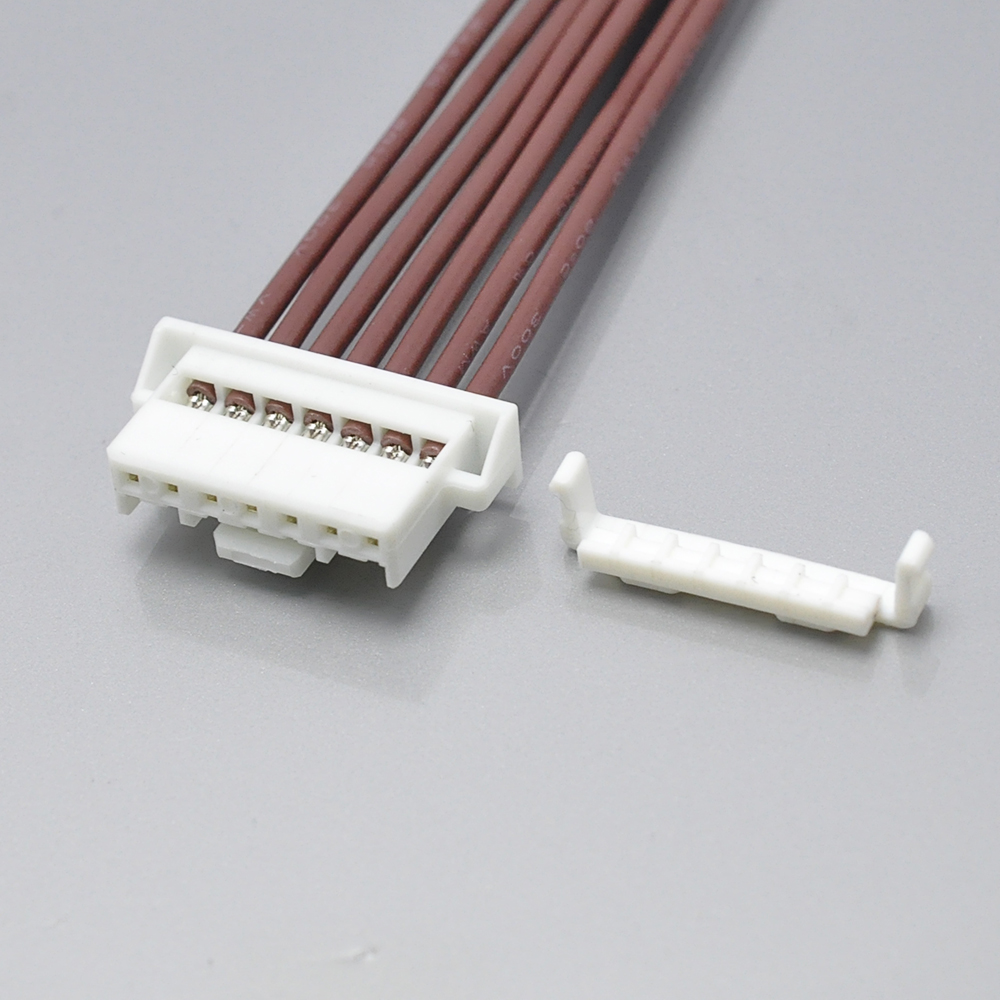
KONNRA KR2022 series PAL 2.0 housing with TPA, the wire-side half of the assembly
8. The environmental programme: eleven tests, one repeated limit
Section 7.0 is the strongest part of this specification, and it is unusually complete for a 2.00mm signal connector.
| Ref | Test | Condition | Acceptance |
|---|---|---|---|
| 7.1 | Durability | 30 cycles at ≤10 cycles/minute (EIA-364-09C) | Contact resistance 40mΩ max |
| 7.2 | Temperature rise | Carrying rated current (EIA-364-70B) | 30°C max |
| 7.3 | Vibration | 1.5mm P-P, 10~55~10 Hz in 1 minute, 2 hours in each of X, Y, Z (EIA-364-28B) | No damage · contact resistance 40mΩ max · discontinuity 1 microsecond max |
| 7.4 | Shock | 490m/s² (50g), 3 strokes in each X, Y, Z axis (EIA-364-27B) | No damage · contact resistance 40mΩ max · discontinuity 1 microsecond max |
| 7.5 | Heat resistance | 125±2°C for 96 hours (EIA-364-17B) | No damage · contact resistance 40mΩ max |
| 7.6 | Cold resistance | −40±2°C for 96 hours (EIA-364-59) | No damage · contact resistance 40mΩ max |
| 7.7 | Humidity | 40±2°C, 90–95% RH, 96 hours (EIA-364-31B) | No damage · contact resistance 40mΩ max · dielectric per 5.3 · insulation resistance 100MΩ min |
| 7.8 | Thermal shock | −40°C for 30 min → room temp 5 min → +125°C for 30 min → room temp 5 min, 5 cycles (EIA-364-32B) | No damage · contact resistance 40mΩ max |
| 7.9 | Salt spray | 35±2°C, 5±1% solution, 24 hours (EIA-364-26B) | No damage · contact resistance 40mΩ max |
| 7.10 | Solderability | 245±5°C for 3±0.5 seconds (EIA-364-52) | 95% of the immersed area free of voids and pin holes |
| 7.11 | Solder heat resistance | SMT against the §9.1 profile (EIA-364-56D); DIP against the §9.2 profile (EIA-364-71B) | Appearance, no damage |
Eight of the eleven state a contact-resistance limit, and all eight allow exactly 40mΩ max — one figure, no split and no carve-out. Against the initial limit of 25mΩ that is a 60% relaxation through conditioning, and it is the number to design against rather than the 25mΩ.
One acceptance limit is much stricter than the initial rating, and it is easy to miss: the humidity test drops insulation resistance to 100MΩ min. The initial requirement in §5.2 is 1,000MΩ min, so §7.7 relaxes it tenfold after 96 hours at 90–95% relative humidity. Neither the product page nor either component page mentions the humidity figure. In a humid application, design against 100MΩ, not 1,000MΩ.
The soldering profiles are qualified separately and correctly:
| SMT infrared reflow (§9.1) | Wave soldering (§9.2) | |
|---|---|---|
| Peak | 255 ± 5°C, 5–10 seconds | 250°C max, 3–5 seconds |
| Time at minimum temperature | 20–40 seconds at ≥230°C | 60–150 seconds at ≥217°C |
| Preheat | 150–200°C, 90–120 seconds | 150–180°C, 60–180 seconds |
The specification’s own note applies and is worth taking literally: “Please check welding conditions by your own devices beforehand. Because the condition changes by the soldering devices, P.C. boards, and so on.” Note also that no reflow cycle count is stated — unlike some original-manufacturer documents, which qualify to a specific number of passes. If your process runs two reflow passes, that is an open question.
Two documentation defects worth raising before you file this specification
The mechanical block in §6.0 contains a wording problem that recurs in this supplier’s documentation, and a signature-block problem in the document as a whole.
Section 6.3 says the terminal retention force is measured by applying “axial pull out force”. Section 6.4 says the pin retention force is measured by applying “axial push force”. Both items measure retention, and a pin-retention test that pushes a post into the wafer cannot measure how hard it is to pull out — the item’s own heading and its requirement (1.2 kgf / 11.76N minimum) only make sense as a pull-out measurement.
I have flagged the same wording in this supplier’s DF3 and PA 2.0 specifications, so it appears to be a template defect rather than a one-off. The practical instruction is straightforward: if you are writing a test procedure from this document, specify pull-out yourself and do not copy the English sentence — particularly for §6.4, where the direction is what the test is measuring.
And the document’s signature block records three fields with two names. Written: Arvin, Checked: /, Approved: Min xinhao. The Checked field is not a name — it is a stroke. For a document that will be cited in a qualification file, that means the independent-check step has no named owner on the record. It is worth asking for the checked revision if you are filing this specification as evidence.
9. What these documents do not publish
Everything below is genuinely absent from the sources reviewed, and is flagged for confirmation rather than estimated. None of it is filled in with a plausible-looking number.
| Item | Status | Why it matters |
|---|---|---|
| Panel thickness | not published | JST’s PAL specifies 0.5mm to 2.0mm for the panel-lock housing; if your design is panel-mounted, that dimension is unqualified on the KONNRA side |
| Free-hanging vs panel-lock variant | not published | JST publishes two PAL housing families — PALR-xxV and PALR-xxVF. KONNRA publishes one housing |
| A second wire-side housing | not published | JST’s PAL is a wire-to-wire connector. The KR2022 set is housing + terminal + wafers, so it documents the wire-to-board use of the PAL housing only |
| Colours | White only | No colour variant, against JST’s fifteen-code colour field |
| Cross-references above 10 circuits | 2 – 10 only | Both cross-reference tables stop at 10, against KONNRA’s own 2–15 component range and JST’s PARP range of 2–13 and 15 |
| Plating thickness | not published | No micron figure for tin, gold or the nickel barrier |
| Creepage and clearance | not published | Frequently a qualification requirement for higher-voltage claims |
| Packaging and reel quantity | not published in the specification | JST publishes 10,000 per reel for SPAL contacts and 1,000 per bag for housings |
| Mating-cycle count for the original | not stated in the JST PA-family document reviewed | KONNRA publishes 30 cycles; the original’s figure was not located, so the two cannot be compared |
| Reflow cycle count | not published | See §9.1 above |
| Agency certificate | UL/USCAR-2 and file E482542 appear on web pages only |
The specification cites no agency file at all — its test methods are EIA-364 series and its only standard reference is UL94 V-0, which is a material flammability rating rather than a listing |
| Wafer dimensions | must be read from the drawing | The KR2022 series drawing is published as vector artwork and its dimensional values are not exposed as machine-readable text |
On the agency row specifically. KONNRA’s housing and terminal pages both state Industry Standard: UL/USCAR-2 | E482542/FTS2304250401. That is a specific UL file number and a reference to USCAR-2, the automotive connector qualification standard — a notable claim for a 2.00mm wire-to-board signal connector. JST’s PA-family document states “Standard: UL” on the PAL series page and refers registration to a separate list, and notes that registered specifications “may differ from the general specifications listed”. Both sides therefore point outside the document for agency evidence, and neither should be filed without the certificate itself.
10. Identification guide: which JST 2.00mm system do you actually have?
Because KONNRA’s title and its part numbers disagree, the most useful thing this article can give you is a three-line test. Your contact prefix is the discriminator, and it is printed on every bag of JST contacts.
| If your housing number begins | And your contact begins | You have | The ratings that apply |
|---|---|---|---|
| PAP- | SPHD- | PA connector, standard type, wire-to-board | 250V AC/DC · −40 to +105°C · contact resistance 10mΩ initial / 20mΩ after test · wire #28–#22 · insulation φ0.76–1.5mm |
| PARP- | SPA- | PA connector, retainer compatible type, wire-to-board | 100V AC/DC · −40 to +105°C · contact resistance 15mΩ initial / 25mΩ after test · wire #26–#22 · insulation φ0.9–1.5mm |
| PALR- (or PALR- with the F suffix) | SPAL- | PAL connector, wire-to-wire, panel lock or free-hanging | 100V AC/DC · −25 to +85°C · contact resistance 15mΩ initial / 25mΩ after test · wire #28–#22 · insulation φ0.9–1.5mm · panel 0.5–2.0mm |
KONNRA’s site lists cross-references for the second row only. The first row is not named anywhere on the KONNRA pages; the third row is named in the product title and in one drawing filename, and its part numbers appear in none of the tables.
So the honest reading of “KR2022 Equivalent To Jst PAL 2.0” is this: the cross-reference is written against the PA retainer-compatible system, which intermates with PAL and shares its 100V rating, and the product is titled after the PAL because that is the name engineers search for. That is a defensible commercial decision. It is not a technical identity, and the differences that follow from it — 100V against 250V, −25 to +85 against −40 to +125, φ0.9–1.5mm against 1.40–1.60mm — are all in the tables above.
One further check, and it is the fastest one. Look at the fourth character group of your contact number. SPHD means standard PA, SPA means retainer-compatible PA, SPAL means PAL. Three letters separate a 10mΩ contact from a 15mΩ one, and four separate it from a different connector entirely. Read it off the reel label before you compare anything else.
11. Where the KR2022 sits, and who it suits
Putting the whole comparison together, the KR2022 is not a like-for-like PAL replacement on paper, and the gap is on the wire side rather than the board side.
It is stronger than the original on three published axes. Rated voltage 250V against 100V. Operating temperature −40 to +125°C against −25 to +85°C. Circuit count up to 15 against 8. If your application is a 4-circuit 24V signal harness that needs a wide temperature window, the KR2022 exceeds the PAL on every published figure that applies.
It is weaker or narrower on four. Contact resistance 25mΩ initial against 15mΩ. Wire range 20–24 AWG against 28–22 AWG, overlapping at two gauges. Insulation window 1.40–1.60mm against 0.9–1.5mm, overlapping in a 0.10mm strip. And it documents one housing against JST’s two PAL housing families, with no panel-thickness figure where JST publishes 0.5–2.0mm.
It is built as a wire-to-board set, and that is the structural difference. JST classifies PAL as wire-to-wire. The KR2022’s documented set — housing, terminal, four wafers — covers the wire-to-board configuration, which JST itself endorses on the PAL page with the remark “Compatible header available (PA connector)”. So if your PAL application is genuinely wire-to-wire, the parts published here do not complete it, and that is the first question to settle.
Who this suits cleanly: a 2.00mm wire-to-board signal design on 22 or 24 AWG with insulation between 1.40 and 1.60mm, where the original was a PA retainer-compatible or PAL part at 100V and the application does not need the panel-lock housing. On that profile the ratings line up, the TPA gives you a secondary-lock check, and the 30-cycle environmental programme is more documented than the original’s catalogue entry.
Who it does not suit: a 26 or 28 AWG PAL harness, a wire with insulation below 1.40mm, a wire-to-wire requirement, a panel-mounted design, or a design budget that assumes 10mΩ or 15mΩ contact resistance.
12. Ten-point cross-reference checklist
- Read your contact prefix first.
SPHD-,SPA-orSPAL-decides which JST rating set applies — 10mΩ, 15mΩ, or a different connector architecture. Section 10. - Measure your wire’s insulation, not its gauge. The KR2022 window is 1.40–1.60mm and JST’s is 0.9–1.5mm. If your insulation is under 1.40mm, this cross-reference is out of range before anything else is discussed.
- Confirm your conductor gauge is 20, 22 or 24 AWG. A 26 or 28 AWG PAL harness has no KR2022 crimp row.
- Quote the rated voltage from the specification, not the page, and expect to justify 250V. JST rates both the PAL and the PARP at 100V AC/DC; the 250V figure matches only the PA standard type, which KONNRA’s pages do not name.
- Carry 800V AC for one minute as the dielectric figure. That is specification §5.3 and it matches JST. The product page’s “250V AC/minute” is the rated voltage in the wrong field.
- Settle the operating temperature in writing. The specification and component pages say +125°C; the product page says +105°C; JST says +105°C for PA and +85°C for PAL. The number your qualification plan inherits needs a source.
- Measure the temperature rise at 3A on your actual gauge. The acceptance limit is 30°C max, and the KR2022 reaches 3A on 24 AWG where JST reaches it on 22 AWG — roughly 37% less copper for the same current.
- Design against 40mΩ, not 25mΩ. Section 7.0 permits 40mΩ max after every environmental test, and humidity relaxes insulation resistance to 100MΩ min from an initial 1,000MΩ.
- Ask for the insulation crimp height on your wire. The table’s 20 AWG figure of 1.30 ± 0.10mm sits at or below the specification’s own 1.40mm minimum insulation diameter, and the ladder runs opposite to the conductor ladder beside it.
- Order wafers by their
C2014...number, and confirm the housing resin. The four wafers in the KR2022 specification carry KR2014 part numbers and the product page links to KR2014 wafer pages; the housing material is PA66/PBT in the specification and PA66 on the page.
13. Frequently asked questions
Is the KR2022 a drop-in replacement for the JST PAL 2.0?
On the ratings, not yet proven; on the part numbers, no. The cross-references published on KONNRA’s pages name PARP housings and the SPA-001T-P0.5 contact, while the genuine PAL parts are PALR- housings and SPAL- contacts. Ratings are a separate question: the KR2022 is published at 250V and −40 to +125°C against the PAL’s 100V and −25 to +85°C, which is higher on both — but the 250V is not traceable to the PAL part it claims to replace, so it needs its own evidence.
Why does the product page say PAL while the components say PARP?
The PA and PAL connectors intermate, and JST’s own PAL page states “Compatible header available (PA connector)”. So a cross-reference written against the PA-side parts can be technically coherent for the multi-connector configuration while the page is titled after the search term engineers use. Treat it as two statements rather than one, and check which one your drawing matches.
What wire can I use?
AWG 20 to 24, on insulation of 1.40 to 1.60mm, per specification §4.0. The crimp table publishes rows for 24, 22 and 20 AWG. Note that the web pages publish only “1.60mm max“, without the 1.40mm floor, and that the housing component page lists a narrower wire range — 22# to 24# — than the terminal page and the crimp table.
What is the voltage rating?
250V AC/DC rated, per specification §4.0 and all three web pages; 800V AC for one minute dielectric, per specification §5.3. The product page’s “Withstanding Voltage 250V AC/minute” contradicts both and appears to be the rated voltage in the wrong field. JST rates the PAL and the PARP at 100V AC/DC and the PA standard type at 250V AC/DC.
How many circuits does it come in?
The documents give four answers: 2-14pin on the product page, 2P~15P on the housing page, 2 to 15 in the specification’s force table, and 2 to 10 in the cross-reference tables. JST’s PAL runs 2 to 8; JST’s PARP runs 2 to 13 and 15, with 14 absent. Configure from a specific part number and get the count confirmed.
Can I get gold plating?
Yes on the terminal and on the DIP wafer contact — no on the SMT wafer contact, which is matte-tin only. The specification states “Tin/Gold over nickel” for the terminal and “Matte-tin/Gold over nickel” for the DIP wafer contact. Neither web page mentions gold at all, so the option has to be quoted from the PDF.
Is the board side really a KR2014 part?
The specification lists all four wafers as C2014VD1****M01**PA and its three siblings, and the product page’s component block links to the four KR2014 wafer pages. The most likely reading is that KR2022 is a wire-side addition to an existing board-side system, but the documents do not state it. Order by the C2014... number and ask the supplier to confirm whether it is the same article as the KR2014 wafer.
How many mating cycles?
30 cycles, per specification §7.1, at no more than 10 cycles per minute, with a post-test contact-resistance limit of 40mΩ max. The force table also publishes the withdrawal force after 30 cycles, which is 0.05 kgf lower than the initial value at every circuit count — a constant absolute loss, not a percentage.
What does the UL number cover?
The housing and terminal pages state UL/USCAR-2, file E482542 / FTS2304250401. The specification itself cites no agency file — its test methods are EIA-364 series and its only standard reference is UL94 V-0, a material flammability rating. Ask for the certificate rather than the web-page line, especially before filing a USCAR-2 claim.
14. Talk to KONNRA about your PAL or PA 2.0 design
If you have read this far, you already know which three questions decide whether the KR2022 fits your design: your wire’s insulation diameter, your contact prefix, and whether your configuration is wire-to-wire or wire-to-board.
Send those three, and KONNRA’s engineering team can tell you in one reply whether the KR2022 is a fit, and if a variant is needed, what it would take:
- Your wire — conductor gauge and measured insulation outside diameter, not the drawing’s nominal figure.
- Your contact prefix —
SPHD-,SPA-orSPAL-, off the reel label. - Your configuration — wire-to-board into a PA header, or a genuine wire-to-wire mate.
- Your circuit count, in part-number form, and your panel requirements if the housing is panel-mounted.
- Your qualification plan — particularly if it cites USCAR-2, in which case ask for the certificate alongside the specification.
You will get back the drawing, the specification, and a crimp recommendation matched to your actual wire — including the insulation crimp height confirmed against the terminal drawing rather than the table in §6.5.
Request a quote or a sample set: konnra.com · product page for this series: KR2022, equivalent to JST PAL 2.0
Sources and method
KONNRA documents. The KR2022 product specification (PS-KR2022-01), revision A01, issued and revised 2023/04/09, 7 pages — cited by section number throughout: §2.0 part numbers, §3.0 materials and surface treatment, §4.0 ratings and applicable wires, §5.1–5.3 electrical performance, §6.1–6.5 mechanical performance including the crimp table, §7.1–7.11 environmental performance, §8.0 insertion and withdrawal force, §9.1–9.2 temperature profiles, §10 remark and signature block. The KR2022 product page (kr2022-equivalent-to-jst-pal-2-0-alternatives-connector) — title, description wording, at-a-glance table, General Specification table, Select Components block and download links. The KR2022 housing component page (components/kr2022-housing) — Features table, cross-reference table, colour and material. The KR2022 terminal component page (components/kr2022-terminal) — Features table, wire range, cross-reference table and the PAL2.0-Terminal.pdf drawing link. Downloads referenced: PS-KR2022-01.pdf, KR2022-series-drawing.pdf, PAL2.0-Terminal.pdf.
JST documents. The PA family catalogue ePA-F (jst-mfg.com/product/pdf/eng/ePA-F.pdf) — the specification blocks for the PA connector standard type, the PA connector retainer compatible type and the PAL connector; the housing, retainer, contact and header ordering tables with their model numbers; and the material callouts. The PAL series page (jst-mfg.com/product/detail_e.php?series=193) — category, panel mounting, lock configuration, circuit range, current and voltage ratings, temperature range, conductor and insulation ranges, and the “Compatible header available (PA connector)” remark.
Method. Every figure in this article is quoted from the sources above; nothing is estimated and nothing is inferred from the shape of a part number. Values that could not be traced to a source are recorded as “not published” in section 9 rather than filled in with a plausible number. The KR2022 force table was extracted from the specification in two different extraction modes because the published table is printed in two halves and the after-30-cycles column is vertically offset from its own rows; both extractions agree value for value once the offset is accounted for, and the resulting table is internally consistent with two exact formulas and one constant. The KR2022 series drawing is published as vector artwork and its dimensional values are not exposed as machine-readable text, so no dimension in this article is quoted from it. Comparisons with the neighbouring KR2014 and KR2009 specifications are made against the same supplier’s published documents for those series. Where a comparison to an earlier series relies on an inference about intent rather than a published statement — the shared wafer part numbers, the identical force table, the inverted insulation-crimp ladder and the shared crimp-strength ladders — it is explicitly labelled as an inference and framed as a question to put to the supplier.