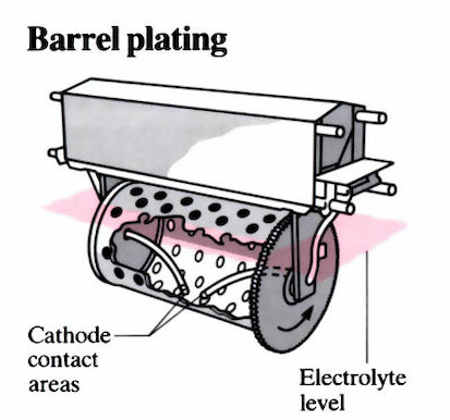
The first type refers to row plating.
Rare metal plating is often required on board edge connectors, board edge protruding contacts, or gold fingers to provide lower contact resistance and higher wear resistance. This technique is called finger plating or bump plating. Gold plating is typically applied to the protruding contacts of board edge connectors with nickel inner layers. The gold fingers or the protruding parts of the board edge adopt manual or automatic plating technology. Currently, the gold plating on the contact plugs or gold fingers has been plated with lead or lead, and is replaced by electroplated buttons. The process is as follows:
1) Strip the coating to remove the tin or tin-lead coating on the protruding contacts.
2) Rinse with clean water.
3) Scrub with abrasive.
4) Soak the activator in 10% sulfuric acid.
5) The nickel plating thickness of the convex contacts is 4~5μm.
6) Clean and remove mineral water.
7) Gold penetration solid solution treatment.
8) Gold plating
9) Clean up.
10) Dry thoroughly.

The second type is through hole plating.
There are various methods to create a desired plating layer on the substrate by drilling the hole walls. This is called pore wall activation in industrial applications. The commercial production process of printed circuits requires multiple intermediate tanks, each of which is called hole wall activation. Tanks have their own control and maintenance requirements. Through-hole plating is a necessary follow-up to the drilling process. As the drill drills through the copper foil and underlying substrate, the heat generated melts the insulating synthetic resin that makes up the base of most substrates. Molten resin and other cuttings accumulate around copper foil holes and coat the newly exposed hole walls, actually being harmful to the surface for subsequent plating. The molten resin also leaves a hot spindle on the substrate hole wall that exhibits poor adhesion to most activators, necessitating the development of a technology similar to decontamination and etch-back chemistry.
A method more suitable for PCB prototyping is to use specially designed low-viscosity ink to form a highly adhesive, highly conductive coating on the inner wall of each via hole. This eliminates the need for multiple chemical treatments and allows a single coating step, followed by thermal curing, to form a continuous coating on the inside of all hole walls that can be plated directly without further processing. The ink is a resin-based substance that is highly adhesive and adheres effortlessly to the walls of most thermally polished holes, eliminating the need for an etch-back step.
The third type is roll-type selective plating.
The pins and pins of electronic components such as connectors, integrated circuits, transistors, and flexible printed circuits are all selectively plated to obtain good contact resistance and corrosion resistance. This plating method can be manual or automatic. It is very expensive to selectively plate each pin individually, so batch soldering must be used. Usually, both ends of the metal foil rolled to the required thickness are punched, chemically or mechanically cleaned, and then selectively made into nickel, gold, silver, rhodium, nickel or tin-nickel alloy, copper-nickel alloy, nickel-lead alloy etc. metal foil. For continuous plating. When choosing this electroplating method, first cover the parts of the metal copper foil board that do not need electroplating with a resist film, and only electroplat the selected copper foil parts.
The fourth type is brush plating.

Another option for electroplating is called “brush plating.” It is an electrodeposition technology. During the electroplating process, not all parts are immersed in the electrolyte. In this plating technology, only a limited area is plated without any impact on the remaining areas. Typically, rare metals are plated onto selected portions of the PCB, such as areas such as edge connectors. Brush plating is more commonly used in electronics assembly shops when repairing discarded circuit boards. A special anode (chemically active anode, such as graphite) wrapped in an absorbent material (cotton swab) is used to transport the plating solution to where plating is required.