In today’s fast-paced technological landscape, the demand for reliable and efficient electronic connectors is ever-growing. This blog post aims to delve into the fascinating world of wafer connectors, a pivotal component in many modern electronic devices. We’ll learn about their definition, structure, working principles, technical characteristics, and the manufacturing process, highlighting insights from KONNRA, a leading electronic connector company.
What Are Wafer Connectors?
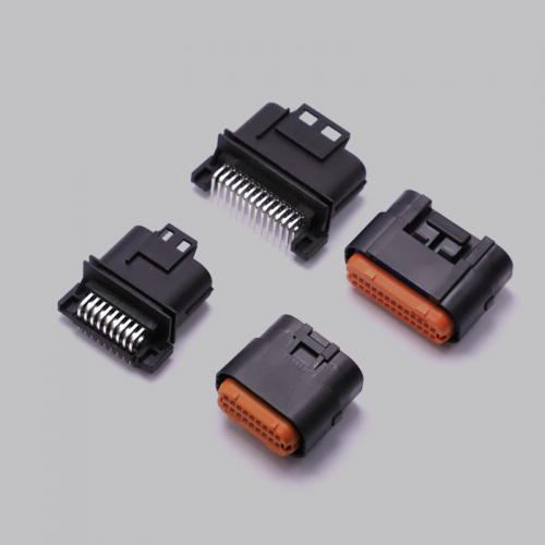
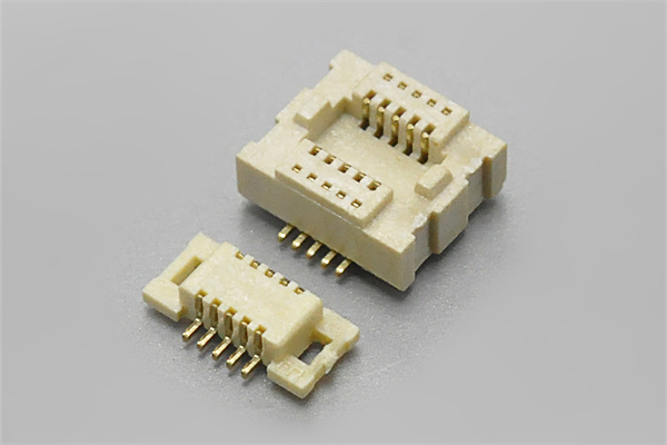
Wafer connectors, also known as board-to-board connectors, are integral parts of electronic systems that enable electrical connections between printed circuit boards (PCBs). These connectors are designed to be compact, allowing for high-density packaging in various electronic devices. The versatility and efficiency of wafer connectors make them indispensable in numerous applications, from consumer electronics to telecommunications and automotive industries.
The primary function of wafer connectors is to facilitate the transfer of electrical signals or power between PCBs. They achieve this by providing a secure and reliable connection point that ensures signal integrity and minimizes the risk of connectivity issues. Wafer connectors come in various shapes, sizes, and configurations, tailored to meet the specific requirements of different electronic applications.
The Structure of Wafer Connectors
Understanding the structure of wafer connectors is essential to appreciate their functionality and advantages. Typically, wafer connectors comprise the following components:
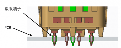
1.Contacts
Contacts are the conductive elements within the connector that ensure electrical connectivity. They are usually made from high-quality metals such as copper or gold, known for their excellent conductivity and resistance to corrosion. The design of the contacts can vary, with options like pin-and-socket or blade-and-receptacle configurations, depending on the application and required connection type.
2.Housing
The housing is the insulating body that holds the contacts in place and provides structural support. It is typically made from durable plastic or other insulating materials that protect the contacts from external elements and prevent electrical shorts. The housing also plays a crucial role in ensuring the proper alignment of the contacts with their corresponding pads or terminals on the PCBs.
3.Locking Mechanism
To ensure secure connections and prevent accidental disconnection, wafer connectors often incorporate a locking mechanism. This mechanism can take various forms, such as latches, snaps, or screws, depending on the design and application requirements. The locking mechanism ensures that the connector remains firmly attached to the PCB, even in environments subject to vibrations or mechanical stress.
How Do Wafer Connectors Work?
Wafer connectors operate by establishing a secure electrical path between two PCBs. The contacts within the connectors align with corresponding pads or terminals on the PCBs, allowing for the flow of electrical signals or power. This alignment and secure attachment are crucial for maintaining signal integrity and device functionality.
When two PCBs need to be connected, the wafer connector provides a straightforward solution. One PCB will have the male part of the connector, while the other PCB will have the female counterpart. When these parts are mated, the contacts within the connector come into contact with the corresponding pads on the PCBs, completing the electrical circuit.
This connection method is not only efficient but also highly reliable, ensuring that the signal transmission remains stable even in demanding environments. The precise design and engineering of wafer connectors ensure minimal signal loss and interference, making them ideal for high-speed data transmission applications.
Technical Characteristics of Wafer Connectors
Wafer connectors offer several technical advantages that make them a preferred choice in many electronic applications. Here are some of the key technical characteristics that set wafer connectors apart:
1.Miniaturization
One of the most significant advantages of wafer connectors is their small size. As electronic devices become increasingly compact, the need for miniature components that do not compromise performance is paramount. Wafer connectors are designed to be small and lightweight, making them ideal for applications where space is limited.
2.High-Density Connections
Wafer connectors allow for a large number of connections within a limited space, enhancing device functionality. Their high-density design enables the integration of multiple connection points in a compact form factor, which is crucial for applications like smartphones, laptops, and other portable devices.
3.Low Contact Resistance
Ensuring efficient electrical conduction is essential for maintaining signal integrity and minimizing energy loss. Wafer connectors are engineered to have low contact resistance, which reduces power loss and heat generation. This characteristic is particularly important in applications that require high-speed data transmission and low power consumption.
4.High Reliability
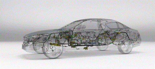
Wafer connectors are designed to withstand environmental stresses, providing durable and long-lasting connections. They are built to resist vibrations, mechanical shocks, and temperature fluctuations, making them suitable for use in harsh environments such as automotive and industrial applications.
5.Versatility
Wafer connectors come in various configurations, allowing for customization based on specific application requirements. This versatility makes them suitable for a wide range of industries, from consumer electronics to medical devices and beyond.
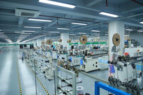
The Manufacturing Process of Wafer Connectors
The manufacturing of wafer connectors involves several precise steps, each crucial to ensuring the final product meets the required standards for performance and reliability. Here’s a detailed look at the typical manufacturing process for wafer connectors:
1.Design and Prototyping
The process begins with the design phase, where engineers create detailed specifications and 3D models of the connector based on the application requirements. This phase involves extensive research and development to ensure that the design meets the necessary electrical, mechanical, and environmental standards.
Once the design is finalized, prototypes are created for testing. Prototyping allows engineers to evaluate the design’s performance and make any necessary adjustments before moving to mass production. This step is critical for identifying and addressing potential issues early in the development process.
2.Material Selection
Selecting the right materials is crucial for the performance and durability of wafer connectors. The contacts are typically made from high-conductivity metals such as copper or gold, which provide excellent electrical performance and resistance to corrosion. The housing is usually made from robust plastic or other insulating materials that can withstand environmental stresses.
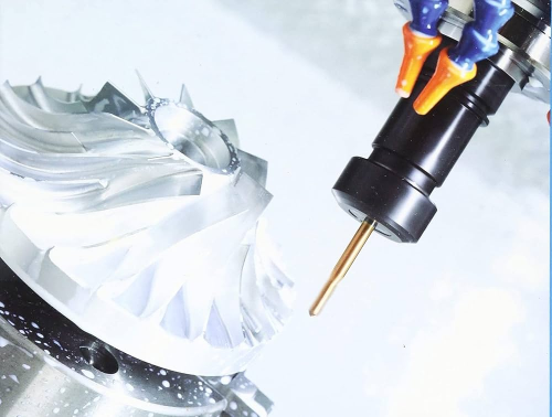
3.Injection Molding
The housing of the connector is typically produced using injection molding techniques. Injection molding involves injecting molten plastic into a mold to create the desired shape. This method allows for high precision and consistency in the production of the housing components.
4.Contact Fabrication
Contacts are stamped or etched from conductive materials and then plated to enhance conductivity and resistance to corrosion. Plating materials such as gold or silver are commonly used to ensure long-term reliability and performance. The contacts are then inspected for quality and consistency before assembly.
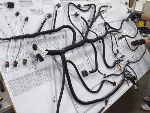
5.Assembly
The assembly process involves inserting the contacts into the housing and adding any additional components such as locking mechanisms. This step requires precision and attention to detail to ensure that the contacts are correctly aligned and securely attached. Automated assembly lines are often used to enhance efficiency and consistency.
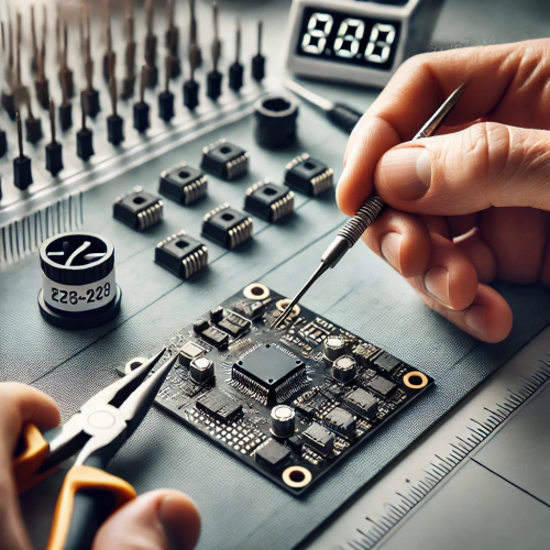
6.Quality Control
Rigorous testing and inspections are performed to ensure each connector meets the required standards. Quality control measures include electrical testing to verify conductivity, mechanical testing to assess durability, and environmental testing to evaluate performance under various conditions. Any connectors that do not meet the standards are rejected and remanufactured.
By following this detailed manufacturing process, companies like KONNRA ensure that their wafer connectors deliver optimal performance and reliability. The commitment to quality and innovation allows KONNRA to provide connectors that meet the demanding requirements of modern electronic applications.
Conclusion
Wafer connectors are a critical component in modern electronic systems, offering numerous technical benefits that enhance device performance and reliability. Understanding their definition, structure, working principles, technical characteristics, and manufacturing process provides valuable insights into their role in the electronics industry. Companies like KONNRA continue to innovate and lead in the development of high-quality wafer connectors, supporting the advancement of technology in various sectors.
By investing in reliable and efficient wafer connectors from trusted connector manufacturers, manufacturers can ensure that their electronic devices meet the highest standards of performance and durability. Whether in consumer electronics, telecommunications, or automotive industries, wafer connectors play a vital role in connecting the future of technology.
In summary, wafer connectors are much more than mere components; they are the unsung heroes that enable the seamless operation of countless electronic devices. With ongoing advancements and a commitment to excellence, the future of wafer connectors looks bright, promising even greater contributions to the ever-evolving world of technology.