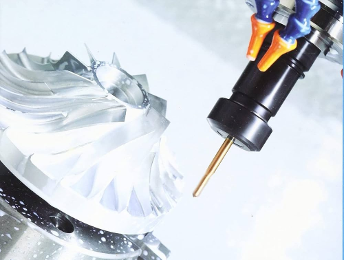
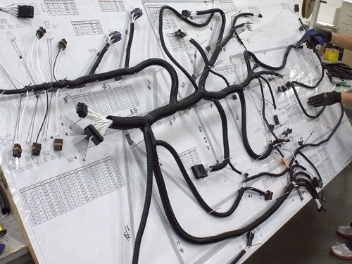
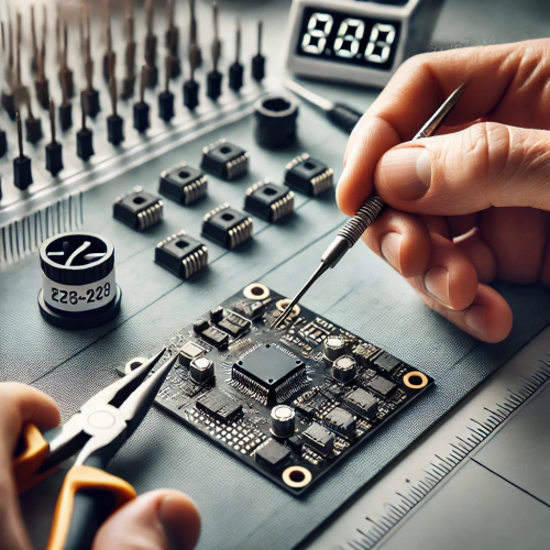
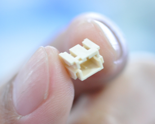
PCB wafer connectors play a central role in the design, assembly and function of printed circuit boards (PCBs). From facilitating electrical connections to improving the reliability and overall performance of electronic systems, wafer connectors are an integral component throughout the PCB life cycle. The following is an analysis of their role from design to function:
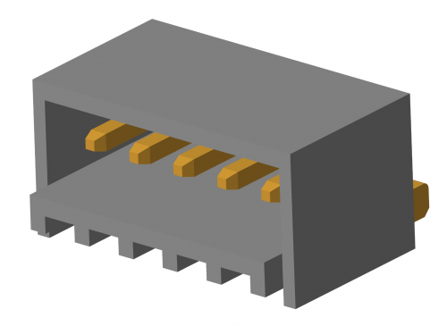
Design phase :
During the PCB design phase, engineers carefully select wafer connectors based on system requirements and integrate them into the layout. Factors such as the number of connections required, space constraints, signal integrity considerations, and environmental factors all influence connector selection.
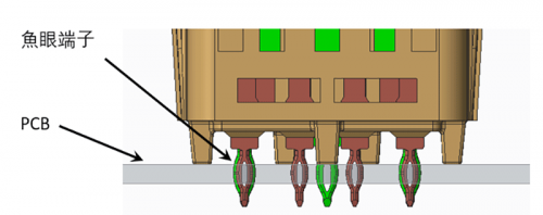
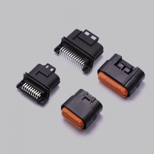
Engineers determine the type, height, and orientation of the wafer connector based on the specific application and PCB layout. They can choose wire-to-board, board-to-board, or wire-to-wire configurations, as well as different termination methods such as surface mount technology (SMT) or through-hole technology (THT).
The placement of wafer connectors on the PCB layout is carefully designed to optimize signal paths, minimize signal interference, and ensure efficient trace routing. Designers also consider accessibility for assembly and maintenance purposes.
Assembly steps :
During the PCB assembly process, the wafer connector is mounted on the PCB using appropriate techniques such as soldering, crimping or surface mounting. The assembly method chosen depends on the connector type, PCB design and manufacturing requirements.
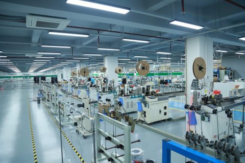
Precision and accuracy during connector placement are critical to ensure proper alignment with PCB pads or holes. Automated assembly equipment can be used to achieve fast and consistent placement of wafer connectors, especially in a mass production environment.
Once the connector is assembled, the wire or cable is terminated to the connector terminals using crimping, insulation displacement or soldering techniques. This step requires skilled assembly technicians to ensure a reliable and secure connection.
Functional stage :
Once assembled, wafer connectors play a vital role in the functionality of PCBs and entire electronic systems. They establish electrical connections between components, subsystems, or external devices and enable signal transmission, power distribution, and data exchange.
Wafer connectors ensure signal integrity by maintaining low resistance and impedance along the signal path while minimizing signal distortion or loss. They also improve system reliability by providing mechanical support and securing the connection against vibration, shock and environmental stress.
In operation, wafer connectors must meet performance specifications for voltage, current, temperature, and environmental conditions to ensure reliable operation throughout the PCB life cycle. They undergo rigorous testing during the quality assurance process to verify their functionality and durability under a variety of operating conditions.
In summary, wafer connectors play a multifaceted role in PCBs, from the design stage when they are selected and integrated into the layout, to the assembly stage when they are assembled and finished, to their functional stage when they enable electrical connections and ensure system performance and reliability. Their importance runs throughout the entire PCB life cycle, making them an indispensable component in modern electronic systems.
In Conclusion
If you are looking for high-quality wafer connectors, our company KONNRA is undoubtedly your best choice. We are committed to meeting all your needs and aim to provide high-quality connector products and high-quality customer service. KONNRA’s customer service team always adheres to the concept of customer first, patiently listens to your needs, and helps you solve any problems encountered during use. Our team members can give you the most satisfactory answer as soon as possible.


